element14 Community
element14 Community
    Register Log In
  • Site
  • Search
  • Log In Register
  • Community Hub
    Community Hub
    • What's New on element14
    • Feedback and Support
    • Benefits of Membership
    • Personal Blogs
    • Members Area
    • Achievement Levels
  • Learn
    Learn
    • Ask an Expert
    • eBooks
    • element14 presents
    • Learning Center
    • Tech Spotlight
    • STEM Academy
    • Webinars, Training and Events
    • Learning Groups
  • Technologies
    Technologies
    • 3D Printing
    • FPGA
    • Industrial Automation
    • Internet of Things
    • Power & Energy
    • Sensors
    • Technology Groups
  • Challenges & Projects
    Challenges & Projects
    • Design Challenges
    • element14 presents Projects
    • Project14
    • Arduino Projects
    • Raspberry Pi Projects
    • Project Groups
  • Products
    Products
    • Arduino
    • Avnet Boards Community
    • Dev Tools
    • Manufacturers
    • Multicomp Pro
    • Product Groups
    • Raspberry Pi
    • RoadTests & Reviews
  • Store
    Store
    • Visit Your Store
    • Choose another store...
      • Europe
      •  Austria (German)
      •  Belgium (Dutch, French)
      •  Bulgaria (Bulgarian)
      •  Czech Republic (Czech)
      •  Denmark (Danish)
      •  Estonia (Estonian)
      •  Finland (Finnish)
      •  France (French)
      •  Germany (German)
      •  Hungary (Hungarian)
      •  Ireland
      •  Israel
      •  Italy (Italian)
      •  Latvia (Latvian)
      •  
      •  Lithuania (Lithuanian)
      •  Netherlands (Dutch)
      •  Norway (Norwegian)
      •  Poland (Polish)
      •  Portugal (Portuguese)
      •  Romania (Romanian)
      •  Russia (Russian)
      •  Slovakia (Slovak)
      •  Slovenia (Slovenian)
      •  Spain (Spanish)
      •  Sweden (Swedish)
      •  Switzerland(German, French)
      •  Turkey (Turkish)
      •  United Kingdom
      • Asia Pacific
      •  Australia
      •  China
      •  Hong Kong
      •  India
      •  Korea (Korean)
      •  Malaysia
      •  New Zealand
      •  Philippines
      •  Singapore
      •  Taiwan
      •  Thailand (Thai)
      • Americas
      •  Brazil (Portuguese)
      •  Canada
      •  Mexico (Spanish)
      •  United States
      Can't find the country/region you're looking for? Visit our export site or find a local distributor.
  • Translate
  • Profile
  • Settings
Robotics
  • Technologies
  • More
Robotics
Blog GIT develops sensor that turns pressure into pixelated light
  • Blog
  • Forum
  • Documents
  • Quiz
  • Events
  • Polls
  • Members
  • Mentions
  • Sub-Groups
  • Tags
  • More
  • Cancel
  • New
Robotics requires membership for participation - click to join
  • Share
  • More
  • Cancel
Group Actions
  • Group RSS
  • More
  • Cancel
Engagement
  • Author Author: Catwell
  • Date Created: 29 Aug 2013 7:40 PM Date Created
  • Views 619 views
  • Likes 0 likes
  • Comments 1 comment
  • research
  • pressure
  • on_campus
  • light
  • embedded
  • cabeatwell
  • prototyping
  • university
  • machine_vision
  • sensor
  • innovation
Related
Recommended

GIT develops sensor that turns pressure into pixelated light

Catwell
Catwell
29 Aug 2013

image

Georgia Institute of Technology’s pressure sensor. (via Georgia Institute of Technology)


We interact with pressure sensors almost on a daily basis, especially when shopping for products, as using a credit or debit card requires signing a pressure sensitive pad (unless those stores still use paper). The problem with checkout pads is that they degrade through repeated use becoming scratched, which requires more pressure to obscurely sign your name. A new development in sensor technology may hold the solution to that problem as well as a host of others, including sensitive skin for robots. Researchers at Georgia Institute of Technology have designed a new pressure-sensitive sensor that mechanically converts pressure directly into light signals that can be optically processed.


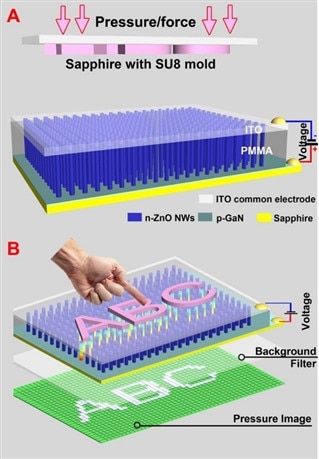
The process of turning pressure into light is known as piezo-phototronics, which generate a charge polarization when under stress. GIT researchers incorporated that process into their newly developed pressure sensor by using thousands of individual zinc oxide nanowires that are chemically grown on top of a gallium-nitride film. When subjected to pressure, the wires produce visible light on the opposite side of the film and the amount of pressure determines the amount of perceived light. When the wires are under strain, they create a piezoelectric charge at both ends of the wire that alters the wires band structure allowing the electrons to remain at the ends of the wire longer. When the nanowires are grouped, they create a form of pixelated light that creates an electroluminescent signal, which can then be read with on-chip photo-optics and transmitted to a computer that can process that information. The incredible thing about their sensor is that it can create up to an astoundinlyg high resolution of 6,300 dpi when using their method of growing the nanowires in a pixelated pattern! The researchers tested their sensor by pressing letters into the top of the film, which in turn displayed the same letters on the opposite side of the film and found it had a response rate of only 90 nanoseconds.


All of the nanowire emitters were able to be seen simultaneously from both sides, which were then tested for 25 on/off cycles in an effort to look for any light degradation and found that the sensor fluctuated in intensity at only 5% of the overall base signal. While the researcher’s sensor is an amazing accomplishment unto itself, the team is already looking for ways to refine their design and upping the resolution even more, which they say could be done by reducing the thickness of the nanowires. This would allow more of the wires to be grown on the film using a higher temperature fabrication process. Besides using their sensor pad for biometrics or signatures at checkout lines, it could be adapted for use as a type of e-skin for robotics that could provide an artificial sense of touch as well as providing a new level of human-machine interface. GIT surmises that the technology could be made commercially available in the next 5 to 7 years, which isn’t very long considering the technology is still in its infancy.


C

See more news at:

http://twitter.com/Cabe_Atwell

  • Sign in to reply
Parents
  • DAB
    DAB over 11 years ago

    Hi Cabe,


    I am dubious that converting the mechanical energy into light is better than the normal electrical impulse generated by the Piezo effect.


    It might be an issue of creating a very small touch sensor, which might have uses in applications where you are looking for minute deformities in a structure or surface.


    I guess I am just skeptical since I have read about "opitical" processing for nearly forty years and have yet to see a usable application.


    Just my opinion,

    DAB

    • Cancel
    • Vote Up 0 Vote Down
    • Sign in to reply
    • More
    • Cancel
Comment
  • DAB
    DAB over 11 years ago

    Hi Cabe,


    I am dubious that converting the mechanical energy into light is better than the normal electrical impulse generated by the Piezo effect.


    It might be an issue of creating a very small touch sensor, which might have uses in applications where you are looking for minute deformities in a structure or surface.


    I guess I am just skeptical since I have read about "opitical" processing for nearly forty years and have yet to see a usable application.


    Just my opinion,

    DAB

    • Cancel
    • Vote Up 0 Vote Down
    • Sign in to reply
    • More
    • Cancel
Children
No Data
element14 Community

element14 is the first online community specifically for engineers. Connect with your peers and get expert answers to your questions.

  • Members
  • Learn
  • Technologies
  • Challenges & Projects
  • Products
  • Store
  • About Us
  • Feedback & Support
  • FAQs
  • Terms of Use
  • Privacy Policy
  • Legal and Copyright Notices
  • Sitemap
  • Cookies

An Avnet Company © 2025 Premier Farnell Limited. All Rights Reserved.

Premier Farnell Ltd, registered in England and Wales (no 00876412), registered office: Farnell House, Forge Lane, Leeds LS12 2NE.

ICP 备案号 10220084.

Follow element14

  • X
  • Facebook
  • linkedin
  • YouTube