Imagine a world where you must tap the silver pads, that have been printed onto your fingers and your thumb, together in a specific pattern to enable the RFID chip that is embedded in your wrist. This is possible because each of the pads on your fingers and thumb is connected via conductive ink that has been tattooed from your fingers to your wrist. This concept could be a reality in the future thanks to research being conducted at Duke University.
The concept of being able to print a soft and flexible circuit, including components, onto human skin as an all-in-one process, has been the topic of biohacking novels and forum posts for years, but such a process has far wider implications than just the cybernetic hackers of the future. While the technology will certainly have a place in security applications, it’s true potential shines when it comes to medicine. Patients of the future could one day have an array of personalized bio-sensors printed onto their skin, allowing their doctor to monitor and record data about that patient’s health over a period of time. This would lead to a more accurate diagnosis and treatment of illnesses and diseases, and its all thanks to Aaron Franklin, the James L. and Elizabeth M. Vincent Associate Professor of Electrical and Computer Engineering at Duke.
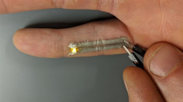
Duke graduate student Nick Williams prints two electronically active leads along the underside of his pinky finger, places small LED light between them and applies a voltage to show the circuit stays intact even when he bends his finger.
Image Credit: Duke University
“When people hear the term ‘printed electronics,’ the expectation is that a person loads a substrate and the designs for an electronic circuit into a printer and, some reasonable time later, removes a fully functional electronic circuit,” said Aaron Franklin. Despite many attempts over the years to develop a process that would allow thin, flexible circuits to be printed-in-place, no one has been able to develop a truly all-in-one process. This new process developed by Franklin and his team claims to be the first to actually produce a truly print-in-place process that is delicate enough for application onto human skin.
The original concept for this type of print-in-place circuit was developed in the late 2000s at the University of Illinois, by John A. Rogers, who is now the Louis Simpson and Kimberly Querrey Professor of Materials Science and Engineering at Northwestern University. Rogers’ version used very thin patches of a flexible rubber that had flexible electronic components already embedded in it. While this concept proved to be revolutionary, it still has it’s drawbacks, such as not being able to modify the circuit on the fly, or quickly scrapping the whole design and quickly starting over again.
“For direct or additive printing to ever really be useful, you’re going to need to be able to print the entirety of whatever you’re printing in one step,” said Franklin. “Some of the more exotic applications include intimately connected electronic tattoos that could be used for biological tagging or unique detection mechanisms, rapid prototyping for on-the-fly custom electronics, and paper-based diagnostics that could be integrated readily into customized bandages.”
Earlier this year, a series of papers was published by Franklin’s team detailing the process and components that make it possible. The first paper detailed a novel ink that contains silver nanowires that can be printed on any substrate at low temperatures using an aerosol-based printer. The result is a thin, highly conductive film that is both flexible, and well adhered to soft substrates such as thin paper and human skin. In fact, the film is able to maintain its conductivity after enduring a 50-percent bending strain more than one thousand times.
In a second paper, graduate student Shiheng Lu and Franklin detail how they use the new conductive ink to print functional transistors. The process starts by the printer deposition a thin strip of semiconducting carbon nanotubes followed by two silver nanowire leads are printed from either side of the carbon nanotube strip. A non-conducting dielectric layer of hexagonal boron nitride is then printed over the carbon nanotube strip with another silver nanowire lead being printed on top of the dielectric layer to act as a gate.
“Nobody thought the aerosolized ink, especially for boron nitride, would deliver the properties needed to make functional electronics without being baked for at least an hour and a half,” said Franklin. “But not only did we get it to work, we showed that baking it for two hours after printing doesn’t improve its performance. It was as good as it could get just using our fully print-in-place process.”
While this process is still in its infancy, and the method originally developed by Rogers is currently moving into mass production, this more personalized method could become the norm one day. For now, it has major potential in one-off applications such as research situations where custom electronics and on-the-fly changes might be required. “Think about creating bespoke bandages that contain electronics like biosensors, where a nurse could just walk over to a work station and punch in what features were needed for a specific patient,” said Franklin. “This is the type of print-on-demand capability that could help drive that.”
Where do you see print-in-place soft circuit technology being in the next 10-years? What applications both medical and none medical do you think would benefit from this technology? I would love to hear about your biohacking ideas that involve this type of circuit. Let me know your thoughts in the comments!
Source: https://pratt.duke.edu/about/news/print-in-place-electronics


Top Comments
-

ralphjy
-
Cancel
-
Vote Up
+3
Vote Down
-
-
Sign in to reply
-
More
-
Cancel
Comment-

ralphjy
-
Cancel
-
Vote Up
+3
Vote Down
-
-
Sign in to reply
-
More
-
Cancel
Children