


 Table of Contents
Introduction
The interfacing to circuits that handle radio frequency (RF) or microwave signals in the Gigahertz (GHz) and tens of GHz range often requires coaxial cables and coaxial connectors. Even if you’re not designing circuits at these high frequencies, you’ll encounter the need to work with RF connectors simply because that’s one of the easiest ways to deliver a signal, for instance from a signal generator, or to an oscilloscope. When it comes to test instrumentation or business or industrial equipment, a reliable and repeatable method may be needed to attach connectors to circuit boards, and the cost of the connector can be insignificant compared to the cost of assembly and testing. This blog (part one of a two- or three-part series) discusses using solderless connectors for this; how they can be used on printed circuit boards (PCBs) to launch RF signals to and from them, and how to design the PCB to suit the connectors. Part two will show the results!
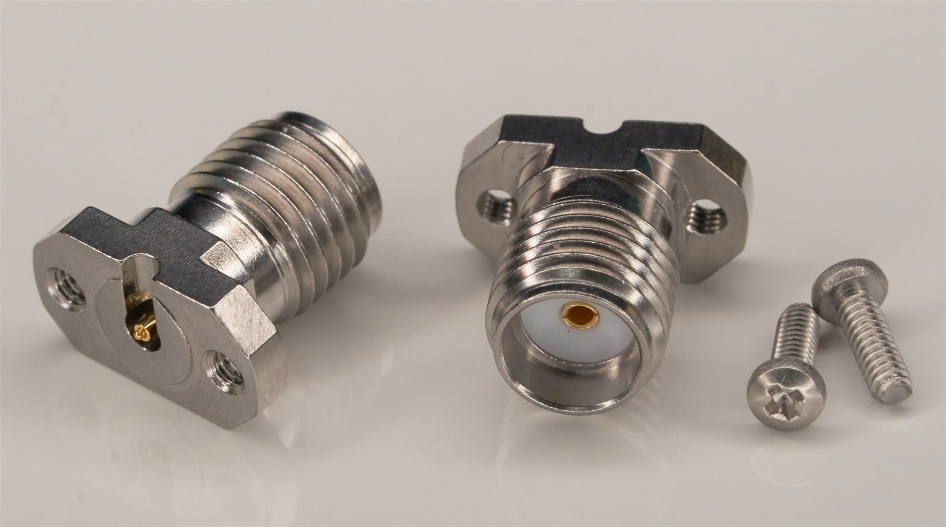
The photo below shows what solderless connectors look like; these are SV Microwave SMA connectors. The underside has a sprung center conductor.
RF Signal Delivery using Transmission Lines
RF signals are often specified in terms of power, and for effective systems, it is important to be able to deliver the power in those signals to the circuit with as little attenuation as possible, and with as little reflection as possible.
RF circuits are often connected using coaxial cables, which are pretty good at delivering signals with no loss (at a first approximation, which is all we are concerned with for now) because the cables look like inductance and capacitance evenly distributed along the length (ignoring resistance, since we are considering just a first approximation), and together the inductance and capacitance appear no different to a real resistance (called the characteristic impedance, often 50 ohms), only until the signal reaches the end of the cable, at which point it is expected that the signal enters the circuit and is absorbed there or further downstream.
The problem is, transitioning from the simple coax cable shape, onto the PCB, requires a certain geometry, so that the inductance and capacitance experience a smooth transition too, maintaining the impedance as smoothly as possible, otherwise, there will be reflections, degrading the signal.
The following formula can be considered (this is an approximation): Impedance = sqrt(L/C)
Therefore, if (say) the capacitance increases anywhere along the signal path, then the inductance needs to be increased there as well, otherwise, the impedance will change, and reflections will result.
Note: Just as an aside, coax and other ways of delivering RF signals, are all known as transmission lines. The name literally derives from the normal power transmission lines used for sending electricity around the country, but at a different frequency.
On a PCB, the predominant way of delivering RF signals (i.e. continuing the purpose of the coax, but on a PCB), is by having a PCB trace and a ground plane nearby, so that the trace inductance and the capacitance to ground are evenly distributed, again so that formula is satisfied with a constant impedance across the length. A few styles are popular, one is called Microstrip, another is called Coplanar Waveguide (CPW), and a variation is called Conductor-Backed Coplanar Waveguide (CB-CPW). Coax offers good shielding, and a PCB transmission line that achieves that is called Stripline, sandwiching the signal between two layers of copper (and flanked with plated via holes).
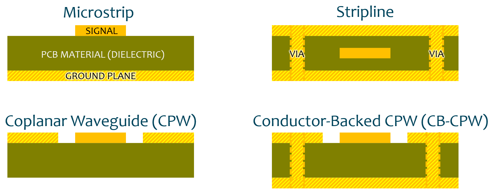
They all have benefits and disadvantages, and there is plenty of documentation on it, but just to discuss a few points, stripline uses up three layers, which could be a disadvantage. It’s also awkward to use since you need a via-hole (not shown in the cross-section diagram above) to pull out the signal onto the surface. CPW and CB-CPW are better in that respect since the trace is on the surface. They still require a lot of via holes though, which makes it hard to use the other side of the PCB for other components.
Incidentally, you can also see the difficulty of soldering connectors in the photo below. The center pin touches a PCB trace that is just 0.35 mm wide in this example, and the center pin is flanked by the large ground connections. An extremely tiny point soldering iron is needed to achieve this without accidentally shorting the pin. A typical soldering iron bit won’t fit through the 1.27 mm gap to even make contact with the pin! The connector needs to be positioned within about 0.1 mm accuracy before soldering.

Although the connections can be just as difficult, at least from the PCB perspective Microstrip is simpler; it requires a ground plane and no via holes, and the ground plane can be an inner layer if desired, meaning that the other side of the PCB can be used for components more easily.
The photo below shows a microstrip trace that can freely be routed around the board provided its width remains constant so that the impedance remains the same throughout. In this example, the signal originates at the left side of the board, and the microstrip is broken up in places for series or shunt components; in total, they happen to form a low-pass filter and the signal egresses from an RF connector on the right side of the photo. The microstrip goes through a curved 90-degree bend overall to get there.

PCB and Layers Selection
For this blog, I was only concerned with using FR4 material, which is the easiest to obtain but is non-ideal for the higher frequency ranges. Even within FR4, there are plenty of options. For instance, using JLCPCB as an example (I will use this throughout as an example, not because I recommend JLCPCB, but because their boards and service are as acceptable as any other typical low-cost prototype PCB supplier; others may be better or worse).
JLCPCB offers a range of options, with not much of an explanation about what they mean. The PDF document from Isola has a bit more explanation. For instance, you can see that the default selection, 7628, has a coarser weave than the next selection that JLCPCB offers (3313). In theory, 3313 would be a better choice, due to the finer consistency, and the lower dielectric constant, and it appears to cost the same. I decided to use 7628, simply because I have used that more often, and I did not wish to experiment with a different material at the same time as experimenting with these new (to me) connectors.
The next question was, what kind of PCB thickness and what layers should be used? In some ways, this was an easy decision because I chose to go with microstrip. A 2-layer 1.6 mm PCB would require a fat trace, ballpark 3mm width (see the photo below for an example of a 2-layer 1.6 mm board). If required, the width can be reduced by using a thinner PCB, or using a 4-layer PCB with the ground plane on an inner layer.

I went with a 4-layer board, because it doesn’t cost that much more than 2-layer boards, and I could use both sides as mentioned, to save a bit of cost there.
Transmission Line Calculations
Some PCB manufacturers try to help with recommended trace widths. For instance, the JLCPCB impedance calculator could be used, although it only offers limited configuration options:

If you were using a different manufacturer that may not have such an online tool, then you can obtain results using software tools such as Saturn PCB Toolkit.
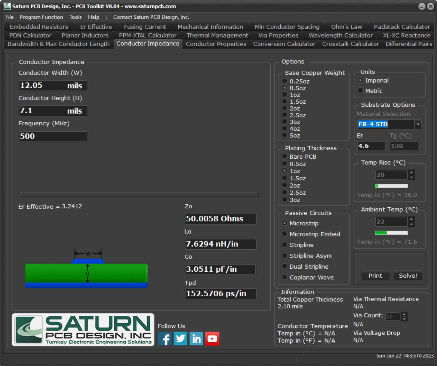
There is a difference of 0.5 mils between the JLCPCB online tool and the Saturn PCB tool; that’s just 0.0127mm.
PCB Layout Elements
The PCB manufacturer will expect CAM (Computer Aided Machining) files, such as Gerber files, in order to create a PCB. The PCB will be designed with a CAD (Computer Aided Design) package.
The render below shows some of the elements that are needed for the final circuit board Gerber files. In the CAD package, some of these elements will be part of the PCB footprint, and others will be part of the PCB layout.
Ideally, the design needs to be easily tunable, because most of the elements and their dimensions will need to be adjusted depending on PCB material and thickness.
Connector Footprint
Just having one connector footprint in your PCB CAD system is not usually sufficient for working with RF connectors, because some things will need to be tuned as discussed above. The main difficulty, as mentioned, is to get the impedance as constant as possible from the connector into the PCB trace. Ordinarily, this requires simulation using software that can cost tens of $k. It would also require training to use the software. This is not practical for a lot of users, and another option is to instead consult the manufacturer to see if they can assist. You’d need to supply detail about your preferred transmission line (for instance microstrip) and board specifications, and then hope the manufacturer can dedicate some time for you. I tried, but I didn’t receive a response after several attempts. I am not a potential customer for more than a few of these connectors, and they might just have larger customers to deal with.
If you have guidelines but do not have a PCB footprint supplied, then you’ll need to create your own because there’s almost zero chance of finding a footprint for these connectors online (until now of course). I used KiCad. The particular connectors are SV Microwave SF2921-61506-1S but there are other options available, both for the connector type and for the intended transmission line type. The SMA connector discussed here is designed for microstrip and coplanar waveguide use.
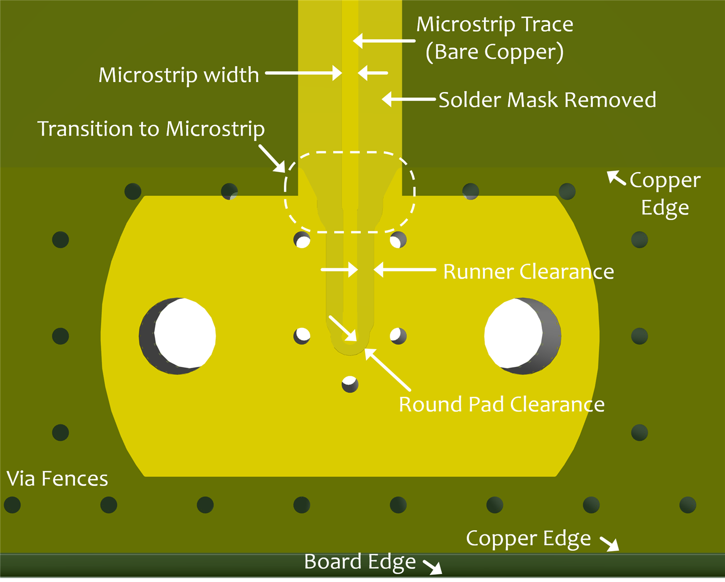
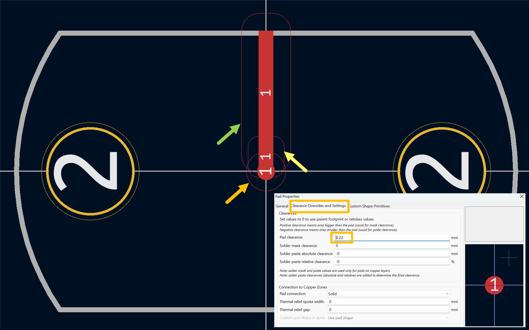
Everyone will have their own way to design footprints. The following screenshot shows one way to be able to control the gap between the conductor and ground plane; After some brainstorming and discussions with Jan Cumps I created two pads, shown with the orange and green arrows below, and numbered them with the same identifier. For each of them, it is possible to set the desired gap (clearance) using the properties dialog as shown in the inset. Next, a third pad (shown with the yellow arrow) is used to bridge the orange and green elements. The yellow arrow shows how the bridging pad provides a way of tuning the clearance transition from the round pad to the stem. Small bridging pads appear to be a convenient solution whenever a portion of the conductor needs its own clearance settings. All this works with KiCad, but if you’re using a different CAD package, then you’ll need to spend time figuring out the best strategy for the tools you’re using.
Finally, a mask layer can be added at the top (and optionally at the bottom). The curved portion of the mask was made in KiCad by setting a very fine grid and drawing point-to-point lines that followed the desired outline. Only a quarter of the mask is drawn in this way, and then it can be copy-pasted three times since there is symmetry in the shape.

If desired, a via fence can be added to the footprint (it saves needing to create it in the PCB layout each time the connector is used). The diameter and spacing depend on the desired maximum frequency of operation; I was only interested in a few GHz operation so I chose slightly larger via holes (0.35 mm) than would ordinarily be expected when using the connector at tens of GHz, and spaced them approximately 2 mm.

PCB Layout
One way to start tuning parameters practically is by creating a test board. A PCB design could be created with many slight variations so that each one can be compared to find the most usable one.
I decided to tune the connector footprint with the following settings; if these settings are very wrong, then I’ll need to create a new board. They are ordered in my best guess order, with SMA_A perhaps being usable, and similarly, the first microstrip width being most likely usable.
SMA Footprints:
| Name | Radius Clearance (mm) | Stem Clearance (mm) |
| SMA_A | 0.22 | 0.35 |
| SMA_B | 0.22 | 0.30 |
| SMA_C | 0.22 | 0.40 |
| SMA_D | 0.27 | 0.35 |
| SMA_E | 0.27 | 0.30 |
| SMA_F | 0.27 | 0.40 |
Microstrip widths:
| Name | Width (mm) |
| MSTRIP_29 | 0.293 |
| MSTRIP_24 | 0.243 |
| MSTRIP_34 | 0.343 |
Test board Connections Summary:
| Group | Reference | Footprint | Microstrip |
| Group 1 | J1-J2 | SMA_A | MSTRIP_24 |
| J3-J4 | SMA_A | MSTRIP_29 | |
| J5-J6 | SMA_A | MSTRIP_34 | |
| Group 2 | J7-J8 | SMA_B | MSTRIP_24 |
| J9-J10 | SMA_B | MSTRIP_29 | |
| J11-J12 | SMA_B | MSTRIP_34 | |
| Group 3 | J13-J14 | SMA_C | MSTRIP_24 |
| J15-J16 | SMA_C | MSTRIP_29 | |
| J17-J18 | SMA_C | MSTRIP_34 | |
| Group 4 | J19-J20 | SMA_D | MSTRIP_29 |
| J21-J22 | SMA_E | MSTRIP_29 | |
| J23-J24 | SMA_F | MSTRIP_29 |
The table above describes the test card; it is shown in the render below.

Half of the design is on the other side since both sides can be used for microstrip, on a 4-layer board:

All of the traces are the same length (approximately 90 mm in my case, since 4-layer boards larger than 100 x 100mm cost more). However, it can be handy to have traces of a different length too, because then it is possible to understand the PCB dielectric constant better (the dielectric constant isn’t actually constant! It varies slightly with frequency). A second test board was also created, again using the same table of connections; the only difference is that the microstrip lengths were shorter. Ideally, this would all be on a single PCB, but that costs a lot more, and I wasn’t willing to do that until a second iteration if needed. This first iteration will be used to try to land in the correct ballpark.

What’s Next?
Once the boards arrive (EDIT: they have arrived! see the photo below), I’ll be in a position to actually send signals down it and see if I can settle on any particular SMA footprint and microstrip width, and then make use of the connector in a project.

One thing I’m especially looking forward to is not having to do any soldering, let alone intricate soldering! This will be a rare project where all that’s required is a screwdriver when the PCB arrives!
I'm also excited about the prospect of reusability. Some test jigs (especially for surface-mount devices) can only be used a few times until they get damaged by SMD pads lifting. I would like to be able to unscrew the connector and move it to a new test board when that happens!
The next blog will follow shortly.
Thanks for reading.


