element14 Community
element14 Community
    Register Log In
  • Site
  • Search
  • Log In Register
  • Community Hub
    Community Hub
    • What's New on element14
    • Feedback and Support
    • Benefits of Membership
    • Personal Blogs
    • Members Area
    • Achievement Levels
  • Learn
    Learn
    • Ask an Expert
    • eBooks
    • element14 presents
    • Learning Center
    • Tech Spotlight
    • STEM Academy
    • Webinars, Training and Events
    • Learning Groups
  • Technologies
    Technologies
    • 3D Printing
    • FPGA
    • Industrial Automation
    • Internet of Things
    • Power & Energy
    • Sensors
    • Technology Groups
  • Challenges & Projects
    Challenges & Projects
    • Design Challenges
    • element14 presents Projects
    • Project14
    • Arduino Projects
    • Raspberry Pi Projects
    • Project Groups
  • Products
    Products
    • Arduino
    • Avnet & Tria Boards Community
    • Dev Tools
    • Manufacturers
    • Multicomp Pro
    • Product Groups
    • Raspberry Pi
    • RoadTests & Reviews
  • About Us
  • Store
    Store
    • Visit Your Store
    • Choose another store...
      • Europe
      •  Austria (German)
      •  Belgium (Dutch, French)
      •  Bulgaria (Bulgarian)
      •  Czech Republic (Czech)
      •  Denmark (Danish)
      •  Estonia (Estonian)
      •  Finland (Finnish)
      •  France (French)
      •  Germany (German)
      •  Hungary (Hungarian)
      •  Ireland
      •  Israel
      •  Italy (Italian)
      •  Latvia (Latvian)
      •  
      •  Lithuania (Lithuanian)
      •  Netherlands (Dutch)
      •  Norway (Norwegian)
      •  Poland (Polish)
      •  Portugal (Portuguese)
      •  Romania (Romanian)
      •  Russia (Russian)
      •  Slovakia (Slovak)
      •  Slovenia (Slovenian)
      •  Spain (Spanish)
      •  Sweden (Swedish)
      •  Switzerland(German, French)
      •  Turkey (Turkish)
      •  United Kingdom
      • Asia Pacific
      •  Australia
      •  China
      •  Hong Kong
      •  India
      •  Korea (Korean)
      •  Malaysia
      •  New Zealand
      •  Philippines
      •  Singapore
      •  Taiwan
      •  Thailand (Thai)
      • Americas
      •  Brazil (Portuguese)
      •  Canada
      •  Mexico (Spanish)
      •  United States
      Can't find the country/region you're looking for? Visit our export site or find a local distributor.
  • Translate
  • Profile
  • Settings
At The Core Design Challenge
  • Challenges & Projects
  • Design Challenges
  • At The Core Design Challenge
  • More
  • Cancel
At The Core Design Challenge
Blog ATCDC: Digimorf, Day 59, The project SEGA SG-1000 Emulator on PSoC62S4 Pioneer kit, part 12
  • Blog
  • Forum
  • Documents
  • Leaderboard
  • Polls
  • Files
  • Members
  • Mentions
  • Sub-Groups
  • Tags
  • More
  • Cancel
  • New
Join At The Core Design Challenge to participate - click to join for free!
  • Share
  • More
  • Cancel
Group Actions
  • Group RSS
  • More
  • Cancel
Engagement
  • Author Author: Digimorf
  • Date Created: 27 Apr 2023 4:21 PM Date Created
  • Views 713 views
  • Likes 5 likes
  • Comments 5 comments
  • ipc
  • PSoC 62S4 pioneer kit
  • modustoolbox
  • dual-core
  • semaphore
  • dma
  • vga
Related
Recommended

ATCDC: Digimorf, Day 59, The project SEGA SG-1000 Emulator on PSoC62S4 Pioneer kit, part 12

Digimorf
Digimorf
27 Apr 2023
ATCDC: Digimorf, Day 59, The project SEGA SG-1000 Emulator on PSoC62S4 Pioneer kit, part 12

Hi to all, welcome back. 

Eight days left, WOW, this time has flown away quickly. I hope you all are where you wanted to be for your project. 

As I knew my project would have presented many obstacles to me, but this is the purpose of a challenge. The next posts will be the last ones, so I will try to show and explain better the techniques that I used to solve problems and exceed the limits where possible. But before I would like to bring your attention to one (potential ?) issue that I am having with the DMA transfer and the SRAM, which is shared by the two cores.

I already explained that my emulator shows the gameplay through a video VGA driver. To do that it needs to render pixels on a video frame buffer, which lives in the SRAM. If I am not wrong, the memory space of the SRAM is always accessible by both cores, except we protect ranges and addresses with the memory protection unit at a low level, or by assigning a range to one core in the linker script at a high level.

That said, I used the core cm0+, clocked at 75MHz, to generate the video, and audio and to handle the Capsense joypad. While I left the cm4, clocked at 150MHz, to run the entire emulation which needs more operative power.

Now, at this point, we understand that the cm0+ has in its domain a frame buffer, and streams pixels stored in it, line by line to the GPIO port interfaced to the VGA monitor through a resistor DAC. But at the same time, the core cm4 needs to generate graphics on that frame buffer, so here the problem comes out.

The VGA driver streams pixels data using a DMAC channel. A pixel clock is used to trig the DMA that for each trig quickly transfers the data from the buffer to the GPIO (@75MHz). The cm4 should render the "next" line in a memory position subsequent to the one used by the VGA driver. In other words, the cm4 prepares the net line to stream by the cm0+.

I have read that the BUS that interfaces the SRAM to the cores and peripherals, has an arbiter that rules the accesses between the different elements. What I didn't expect is that the DMA seems NOT having priority over normal access by a core ( buffer[x] = byte, I mean).

I was able to notice this because one pixel, at a resolution of 256 pixels in width, is 95ns wide. this means that a small delay in accessing the memory by the DMA is absolutely visible on the monitor.

DMA and memory access interferences

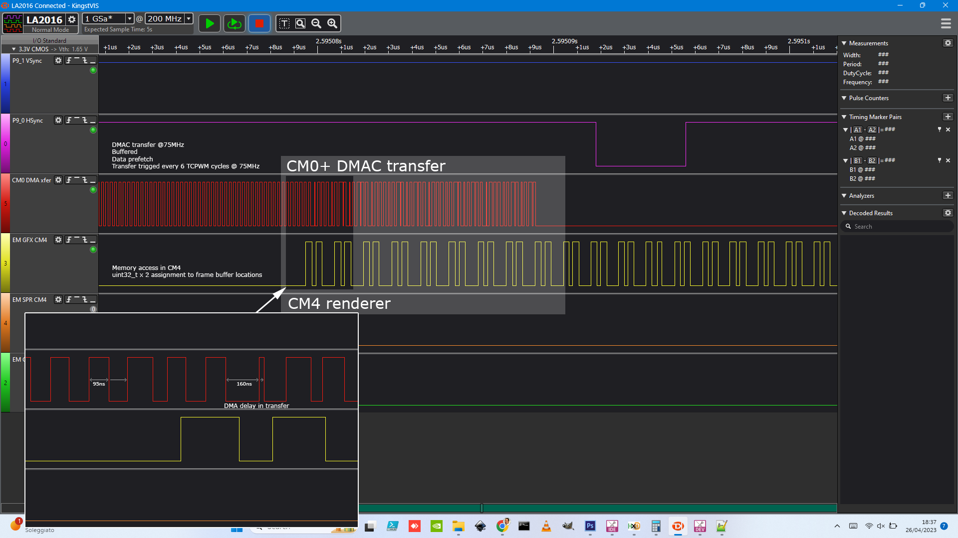
In this snapshot taken from the Logic Analyzer, is shown how the DMA transfer (Red) is affected by memory location assignment by the cm4 (yellow). 

The result is a noisy image on the screen. I have worked hard to try to coordinate this access, but it is almost impossible to use IPC since the DMA can't pause the cm4, and the renderer in the cm4 eats a lot of cycles while rendering graphics and running the emulated CPU (Z80).

The best I could do is to instruct the VGA driver to show even lines and leave the odd lines black. This creates a nice old-fashioned CRT effect and leaves time for rendering graphics by the cm4 in peace without showing a shacked scanline. Another trick I used is to render graphics in between the shown scanlines and to emulate the virtual machine in the "Blank" area of a video frame at the bottom of the video frame.

image

This looks better, and it was possible by using memory-mapped registers instead of IPC. In other words, both cm0 and cm4 write/read a specific memory location and act accordingly.  Like semaphores of IPC but faster and without interrupts.

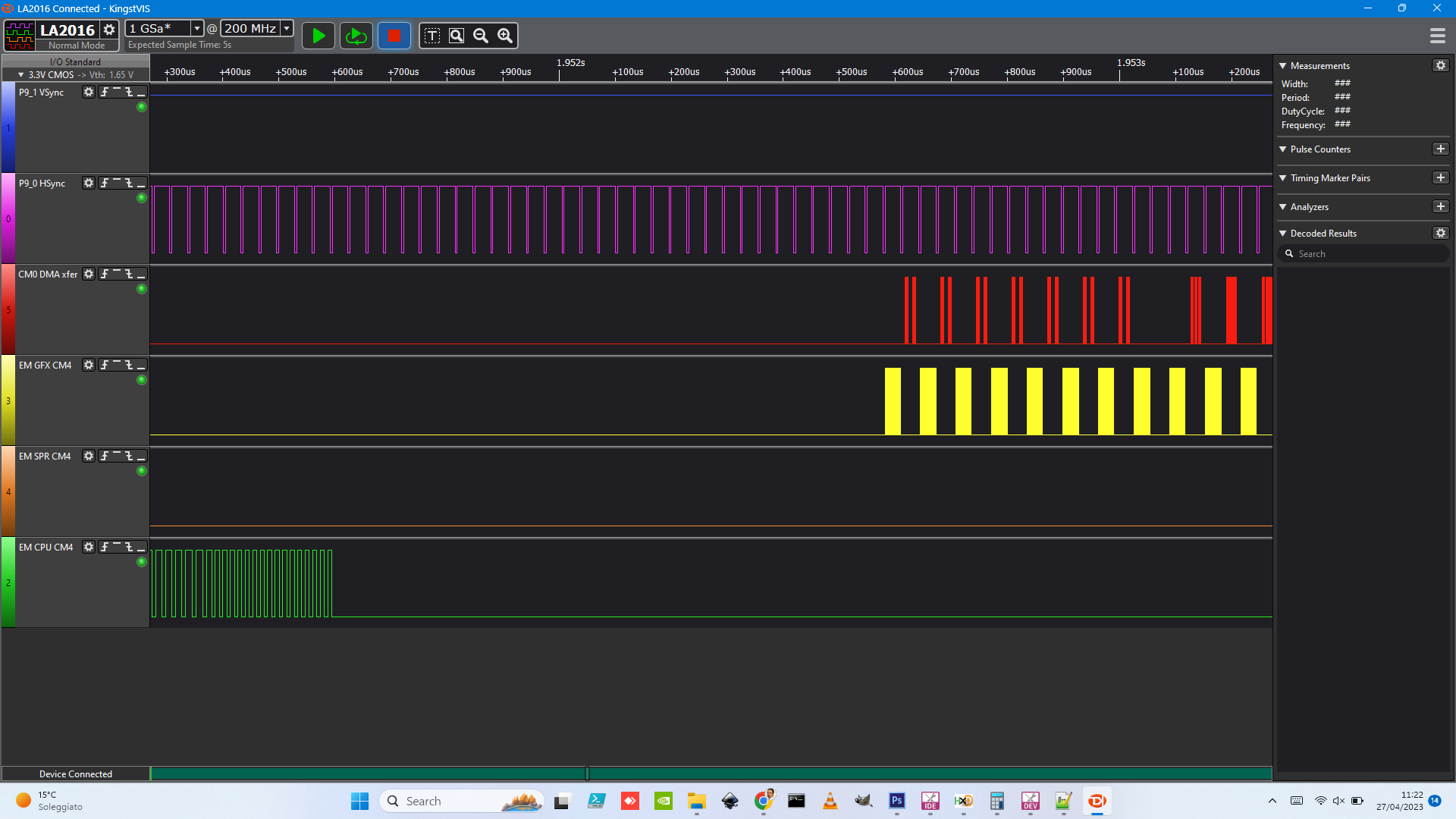
The two next snapshots show the difference between toggling a GPIO using a shared memory location and using an IPC semaphore, please correct me if I am doing something wrong Wink.

// cm0+
    for (;;)
    {
#if 0
      _SHARED_gCommand = 1;
      GPIO_PRT10->OUT |= 1;
      while (_SHARED_gCommand) {};
#else
      Cy_IPC_Sema_Set(16, false);
      GPIO_PRT10->OUT |= 1;
      while (Cy_IPC_Sema_Status(16) == CY_IPC_SEMA_STATUS_LOCKED) {
      }
#endif
    }

// cm4
    for (;;)
    {
#if 0
      while (_SHARED_gCommand == 0) {};
      _SHARED_gCommand = 0;
      GPIO_PRT10->OUT &= 0xFE;
#else
      while (Cy_IPC_Sema_Status(16) == CY_IPC_SEMA_STATUS_UNLOCKED) {
      }
      GPIO_PRT10->OUT &= 0xFE;
      Cy_IPC_Sema_Clear(16, false);
#endif
    }

Shared memory:

image

IPC semaphore:

IPC semaphore toggle pin

In any case, even if the two processes are synchronized as shown, there are still problems as long as there is access to the SRAM. 

That said, if I am not wrong, this is an issue for real-time projects or when there are tight timings. while for graphics It's possible to use a TFT module since many controllers have their own frame buffer. But if you want a VGA or a Video composite signal, things can become difficult. 

The next posts will be the conclusion of this adventure.

  • Sign in to reply

Top Comments

  • ljking
    ljking over 2 years ago +1
    Hi @digimorph Sorry for the delay. I did some research on this topic. Each SRAM block has two ports, a High Speed port, and a Low Speed port. The bus masters on each port have a 'priority' which is set…
  • Digimorf
    Digimorf over 2 years ago

    Hi, I had some time to spend in R&D yesterday, and I tried to investigate the jitter caused apparently by the access to the SRAM at the same time by the cores.

    I have plug this "PSoC6 Gaming System" (Iam making fun of it) to my big TV and I noticed that the jitter involves the starting point of the scanline, since it seems that it translates randomly when things in the game moves heavily. So it's the entire line that translates, not single pixels. All this things suggest me that the DMA transfers are not really affected by the arbitration, otherwise the line would have been shrink or stretched irregulairly. Maybe something happens when the Inerrupt of the scanline fires.

    This sounds weird to me because the two cores have two indipendent interrupt systems. But wait, the vector table is located into the SRAM! The startup code *.s takes care of copying the table from Flash to SRAM. So, is it possible that the jump action to the ISR location is influenced by a delay during the fetching of the address from the vector table in the SRAM? 

    I should leave  the table in the Flash, but it seems a bit tricky because all the memory map in the linker file is designed accordingly to the vector table located in the SRAM.

    Probably I will work more on it in the next days for fun, but I wanted to bring your attention to this potential issue for a dual-core design. 

    • Cancel
    • Vote Up 0 Vote Down
    • Sign in to reply
    • More
    • Cancel
  • Digimorf
    Digimorf over 2 years ago in reply to ljking

    Thank you for your support, very helpful.

    Actually, the MPU ansi SMPU aren't that clear, I tried to examine the PDL library and there are specific functions for the configuration of those units. 

    Unfortunately there is no time left for improvement now, so I will continue this project after the end of the competition. Moreover the project doesn't require any special hardware to be replicated for those who want to work on it later, so it could become a starting point for other projects. 

    The truth is that this MCU is surprising me day by day.  So this experience has been very positive.

    • Cancel
    • Vote Up 0 Vote Down
    • Sign in to reply
    • More
    • Cancel
  • ljking
    ljking over 2 years ago

    Hi @digimorph

    Sorry for the delay. I did some research on this topic. Each SRAM block has two ports, a High Speed port, and a Low Speed port. The bus masters on each port have a 'priority' which is set in the PROT_SMPU_MSx_CTL[PRIO] registers described in the Technical Reference Manual (TRM). What is missing from the TRM/Datasheet is the mapping of 'x' to the various bus masters. Here is the mapping for 'x' and the bus masters:

    0 - CM0+

    1 - Crypto

    2 - DW0

    3 - DW1

    4 - DMA

    5 - DW0 (slow)

    6 - DW1 (slow)

    14 - CM4 (cortex M4)

    16 - DAP (debug)

    In your case I 'think' you need to change the priority in the PROT_SMPU_MS4_CTL[PRIO] register, but I haven't tried it so I am not positive this will work.

    • Cancel
    • Vote Up +1 Vote Down
    • Sign in to reply
    • More
    • Cancel
  • Digimorf
    Digimorf over 2 years ago in reply to dougw

    Correct, but since the PSoC62s4 is dual-core, the embedded SRAM controller should be configurable or should give priority to the DMA, which can run in the background. Again, no problem if the timings in the applications aren't a problem.

    • Cancel
    • Vote Up 0 Vote Down
    • Sign in to reply
    • More
    • Cancel
  • dougw
    dougw over 2 years ago

    It sounds like you need dual port RAM...

    • Cancel
    • Vote Up 0 Vote Down
    • Sign in to reply
    • More
    • Cancel
element14 Community

element14 is the first online community specifically for engineers. Connect with your peers and get expert answers to your questions.

  • Members
  • Learn
  • Technologies
  • Challenges & Projects
  • Products
  • Store
  • About Us
  • Feedback & Support
  • FAQs
  • Terms of Use
  • Privacy Policy
  • Legal and Copyright Notices
  • Sitemap
  • Cookies

An Avnet Company © 2025 Premier Farnell Limited. All Rights Reserved.

Premier Farnell Ltd, registered in England and Wales (no 00876412), registered office: Farnell House, Forge Lane, Leeds LS12 2NE.

ICP 备案号 10220084.

Follow element14

  • X
  • Facebook
  • linkedin
  • YouTube