element14 Community
element14 Community
    Register Log In
  • Site
  • Search
  • Log In Register
  • About Us
  • Community Hub
    Community Hub
    • What's New on element14
    • Feedback and Support
    • Benefits of Membership
    • Personal Blogs
    • Members Area
    • Achievement Levels
  • Learn
    Learn
    • Ask an Expert
    • eBooks
    • element14 presents
    • Learning Center
    • Tech Spotlight
    • STEM Academy
    • Webinars, Training and Events
    • Learning Groups
  • Technologies
    Technologies
    • 3D Printing
    • FPGA
    • Industrial Automation
    • Internet of Things
    • Power & Energy
    • Sensors
    • Technology Groups
  • Challenges & Projects
    Challenges & Projects
    • Design Challenges
    • element14 presents Projects
    • Project14
    • Arduino Projects
    • Raspberry Pi Projects
    • Project Groups
  • Products
    Products
    • Arduino
    • Avnet Boards Community
    • Dev Tools
    • Manufacturers
    • Multicomp Pro
    • Product Groups
    • Raspberry Pi
    • RoadTests & Reviews
  • Store
    Store
    • Visit Your Store
    • Choose another store...
      • Europe
      •  Austria (German)
      •  Belgium (Dutch, French)
      •  Bulgaria (Bulgarian)
      •  Czech Republic (Czech)
      •  Denmark (Danish)
      •  Estonia (Estonian)
      •  Finland (Finnish)
      •  France (French)
      •  Germany (German)
      •  Hungary (Hungarian)
      •  Ireland
      •  Israel
      •  Italy (Italian)
      •  Latvia (Latvian)
      •  
      •  Lithuania (Lithuanian)
      •  Netherlands (Dutch)
      •  Norway (Norwegian)
      •  Poland (Polish)
      •  Portugal (Portuguese)
      •  Romania (Romanian)
      •  Russia (Russian)
      •  Slovakia (Slovak)
      •  Slovenia (Slovenian)
      •  Spain (Spanish)
      •  Sweden (Swedish)
      •  Switzerland(German, French)
      •  Turkey (Turkish)
      •  United Kingdom
      • Asia Pacific
      •  Australia
      •  China
      •  Hong Kong
      •  India
      •  Korea (Korean)
      •  Malaysia
      •  New Zealand
      •  Philippines
      •  Singapore
      •  Taiwan
      •  Thailand (Thai)
      • Americas
      •  Brazil (Portuguese)
      •  Canada
      •  Mexico (Spanish)
      •  United States
      Can't find the country/region you're looking for? Visit our export site or find a local distributor.
  • Translate
  • Profile
  • Settings
Experimenting with Flyback Transformers
  • Challenges & Projects
  • Design Challenges
  • Experimenting with Flyback Transformers
  • More
  • Cancel
Experimenting with Flyback Transformers
Blog DC to DC Demystified - Blog 1 - Does it fly back?
  • Blog
  • Forum
  • Documents
  • Polls
  • Files
  • Members
  • Mentions
  • Sub-Groups
  • Tags
  • More
  • Cancel
  • New
Join Experimenting with Flyback Transformers to participate - click to join for free!
  • Share
  • More
  • Cancel
Group Actions
  • Group RSS
  • More
  • Cancel
Engagement
  • Author Author: Anthocyanina
  • Date Created: 10 Jan 2024 11:02 PM Date Created
  • Views 2502 views
  • Likes 11 likes
  • Comments 21 comments
  • flyback converter
  • smps
  • EXPERIMENTING WITH FLYBACK TRANSFORMERS
  • SMPS Flyback Transformers
  • bourns
  • dc to dc
Related
Recommended

DC to DC Demystified - Blog 1 - Does it fly back?

Anthocyanina
Anthocyanina
10 Jan 2024
Group photo!

This being my first blog, i'll begin with a short introduction:

My name is Sara, I'm an electronics engineering student and electronics is also my hobby, I came across the element14 community when looking for help with a function generator, and have continued to visit it occasionally as it has proved to be a valuable source of knowledge and fun content.

When I started in electronics, adventuring into power electronics felt a bit scary, and when it came to switched-mode power supplies, I just wanted to avoid them, even at the cost of efficiency and space.

It seems many newcomers to the world of electronics also find them at least a bit confusing, so I'll try my best to remove the mystery around designing your own switched-mode supply, in this case, around the flyback topology.

This series of blogs will assume you have some basic understanding of how inductors work, and what a transformer is.

With that out of the way, let's get to it, first,

Meet the family!

Thanks to element14 and Bourns for providing a fairly comprehensive transformer kit. This kit contains all the magnetic components you'll need to build a proper power supply: Gate driver transformers(in green), Flyback transformers, and common mode chokes(in red).

Bourns's design challenge kit

And that's it? Won't you tell us more about them? Well, rather than going into detail about each transformer in this blog, I'm just going to jump right into building a circuit and see what happens!

I thought it would be easiest to start with the lowest input voltage transformer:

The BA60951CS

today's subject of focus

This is a really tiny transformer

 they really are tiny!

Bourns has made this really compact transformer to work with an input voltage between 7 and 24V and rated the secondary to 15V. Perfect to work with at the bench. They specified the working frequency of this transformer to be 120KHz, but the electrical specifications were, well, specified at 250KHz. Because of this, I'll be using a switching frequency of 250KHz, especially since it's also here that its Q factor approaches its maximum of around 70 when measuring it with an impedance analyzer. This tells me that the 120KHz working frequency is likely a mistake in the datasheet.

 primary inductances and Q factor measurements

With the impedance analyzer we can of course also measure the leakage inductance, which is the inductance that isn't magnetically coupled to the other windings of the transformer, but instead acts as if we added an inductor in series to an ideal transformer.

To measure the leakage inductance, we short all the windings, except the one we want to measure:

This is only correct if we're using all the windings. To properly measure the leakage inductance, connect the winding to measure, and short the other windings you will use. If you are only going to use two windings from a transformer with 3 or more, leave the rest unshorted. At the end of the post, there will be a link to a video by Biricha showing how to properly measure a transformer. Thanks to javagoza for pointing this error out.

 test setup for measuring leakage inductance

Knowing what this leakage inductance is will be useful later when it's time to design the snubber circuit, because this inductance, together with the parasitic capacitance of our switch will determine the ringing frequency during the off portion of the flyback cycle, and knowing this frequency wll inform the component selection for our snubber. If you have no idea what a snubber is, or why a flyback cycle has an off portion, don't worry, we'll get to that in the next blog.

Inductance and leakage inductance masurement results

Bourns says in the datasheet that this transformer has a nominal primary inductance of 25 µH, a nominal leakage inductance of 0.6 µH, and a primary DC resistance of at most 0.55 ohms, and this is confirmed by the measurements with values of 24.75 µH, 450nH, and 553 milliohms, respectively. They also provide us with the turns ratio between primary and secondary of 0.77, and from the equation that connects turns ratio with inductance:

 image

we input the inductances:

image

and get a turns ratio of 0.7696, almost exactly what the datasheet claims. Perfect!

now let's take a look at

The Flyback converter topology

flyback converter schematic with mostly ideal components

This is the simplest flyback converter schematic representation, and in this case, the components used are all ideal, except for the MOSFET, as I couldn't get LTspice to run a proper simulation with an ideal voltage controlled switch. The selection of the MOSFET and that of the other components is such just because those were the components I had lying around, it was random, and after all, this was just meant to be a proof of concept, to see if the circuit would work.

Using this almost ideal schematic, we can see how the voltage output equation for a flyback converter (in DCM mode) gives us a close match to what we see in the simulation, where R is the load resistor, T is the period of our switching frequency, D is the duty cycle, and Lp is the primary inductance (primary inductance for the ideal case only):

image

 a look at the input and output voltages

Lp should technically be the magnetizing inductance, but for now, as the modeled transformer is ideal, the entire primary inductance is assumed to be magnetizing.

After seeing the simulation results, I went to build the circuit:

flyback converter on a breadboard, 10 ohm sense resistors are paralleled with jumpers, to use either of them depending on what's being measured

 a look at the MOSFET and output stage of the converter

I also added 10 ohm resistors in series with both the input and the output to take a look at the currents, which according to the (close to) ideal simulation should look like this: 

 a simulation of the almost ideal circuit, showing the primary current and output diode current

(that ringing on the primary side current has to do with parasitic components in the mosfet, which we'll see later)

but since my real life components are far from ideal, I went ahead and measured everything using the impedance analyzer, and then modeled the circuit in LTspice as well as my measurements allowed me to, and now the current waveforms became spicier: 

 primary and diode currents with more realistic components

you might also notice that the transformer coupling is no longer 1. This is because with real components we have less than perfect coupling, and the uncoupled part is what becomes the leakage inductance. 

We can calculate the coupling factor like this:

image

This equation also assumes no losses, but if we model the transformer as measured, ideally coupling the magnetizing inductance and adding the leakage inductance in series, uncoupled, as well as taking into account the series resistance of the windings, we get a very similar result, just with larger amplitude ringing as you can see here:

image

now let's take a look at the MOSFET and diode currents in the real circuit:

 a real measurement of the circuit, with the jumpers across the 10 ohm resistors removed

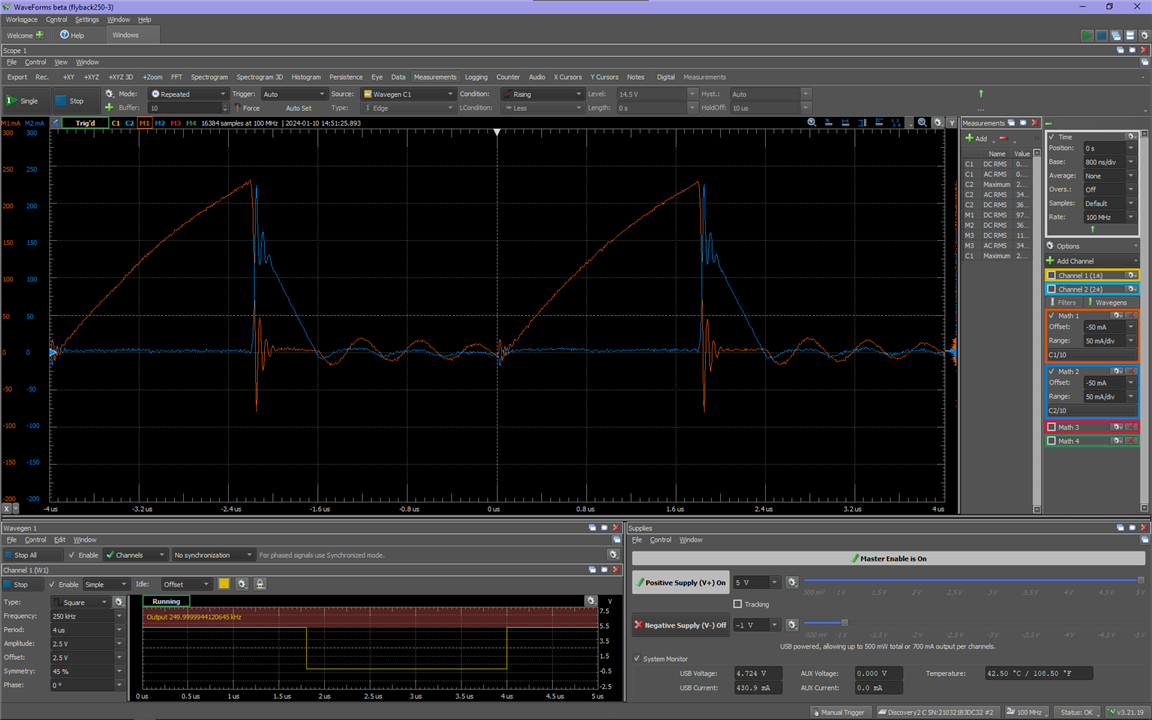
we can see that they are an almost exact match to what we see in the simulation. From this we can now safely assume that the circuit will behave just as in the simulation once i bridge the 10 ohm resistors. We won't be able to see the currents anymore, but knowing that the circuit behaves just as expected from the simulation, we can use the results of the resistorless simulation, together with the voltage measurements of the real life circuit to get the complete picture of what's going on with our circuit.

So, does it fly back?

Well, from this experiment we can see that this simple converter cobbled together from an assortment of randomly selected components does behave exactly as seen in the diagrams found all over the internet which show the waveforms of a DCM flyback converter. It does fly back!

But what exactly is it that *flies back*?

While the circuit's behaviour is almost textbook, and that's great! it is still not entirely clear to me what flies back, having found different answers in different places, with some saying that "flyback" refers to the beam in CRT TVs flying back to where it would begin drawing the next line, others saying it is about the energy "flying back" from one winding to the other on the off portion of the cycle, and others saying it is about the magnetic field collapse in the transformer.

Another explanation which seemed pretty reasonable is that when it came to the CRT high voltage transformers, they got their name because if you touched one live, it would make you fly back! Wink

Anyway, seeing how easy it is to get a flyback converter going was very encouraging, and since this cobbled together circuit worked perfectly, I'm going to continue exploring the flyback topology on it. 

In this image from TI's "Power Tips #98: Designing a DCM flyback converter" PDF, we see all the waveforms we should expect to see, as well as the ones we actually saw.

image

but there is one important waveform left we have yet to look at, the voltage at the MOSFET (Voltage between Drain and Source). Let's take a look:

 in green: Vds of our almost ideal circuit

On this almost ideal circuit, we see it is just as expected, with the maximum Vds of around 20.5V, which would be what we get from the equation described in TI's guide:

image

and from our closer to real life simulation:

 in green: Vds of our more realistic circuit

well, that is *not ideal* for sure! we're getting spikes of over 25V at Vds!

and our real life circuit, again, agrees with the simulation: 

 Vds of our real life circuit

so, what is going on here? That's what I'll explore in the next blog, what that ringing is, where does it come from, why do we not want it, and how to get it under control. Here's a sneak peek at how that looks like when it's under control:

 voltage spikes under control, but how? hmmm!

Again, this is my first blog, and I'm far from being a writer, so I'm also taking this as an opportunity to ask for feedback, let me know what you think I can improve about my writing, so the next blogs are nicer to read.

Any questions, I'll be happy to answer in the comment section.

Thank you! Slight smile

How to properly measure transformers: Transformer Measurements

  • Sign in to reply

Top Comments

  • Anthocyanina
    Anthocyanina over 1 year ago in reply to Anthocyanina +1
    I couldn't wait to post this in another blog, so the simulations here will also serve as sneak peeks: This is how the currents look like with the unshorted aux leakage measurement, this looks the furthest…
  • javagoza
    javagoza over 1 year ago in reply to Anthocyanina

    Thanks to you. It's really nice when participants post regularly and delve deeper into their learnings. I prefer slow food. You are making an excellent series of posts and the simulations help a lot to understand what is happening underneath.

    • Cancel
    • Vote Up 0 Vote Down
    • Sign in to reply
    • More
    • Cancel
  • Anthocyanina
    Anthocyanina over 1 year ago in reply to javagoza

    Can't believe I didn't hit send when i wrote a reply to this. Thank you javagoza, measuring at the ringing frequency, and with the windings to be used is indeed how it should be done, and while the measurement procedure is the same, the value obtained at the ringing frequency will be lower. One interesting thing about this is that by performing the measurement with the other winding (or windings, depending on which ones you will use) you're also getting the value for the referred leakage of that winding, so you can perform the measurement on just one side to then calculate the snubber.

    image

    Here you see the frequency and amplitude of the spike and ringing at vds are almost identical in both circuits. not being the same because of measurement error. (ignoring that these are the values obtained at 250KHz and not the ringing frequency) So measuring leakage on one winding really is enough!

    Thanks again! Slight smile

    • Cancel
    • Vote Up 0 Vote Down
    • Sign in to reply
    • More
    • Cancel
  • jc2048
    jc2048 over 1 year ago in reply to shabaz

    If it helps, this is from Television Servicing for Beginners (1956). That's a simplified circuit to give an idea of the principles. So this does suggest a path to 'flyback' getting attached to the method where some kind of transformer action is added to a ringing choke.

    image

    image

    image

    • Cancel
    • Vote Up 0 Vote Down
    • Sign in to reply
    • More
    • Cancel
  • javagoza
    javagoza over 1 year ago in reply to Anthocyanina

    Thank you for taking so much interest in the response, you actually have enough there for another blog, cheer up.


    That 14.44 MHz frequency is above the frequencies that the Analog Discovery 2 can measure, it will not be possible to measure the inductance with that impedance analyzer.

    In some of the tests that I did with other transformers at the ringing frequency, the leakage inductance was already decreasing with the frequency instead of increasing. It may not be your case.

    image

    • Cancel
    • Vote Up 0 Vote Down
    • Sign in to reply
    • More
    • Cancel
  • Anthocyanina
    Anthocyanina over 1 year ago in reply to javagoza

    About measuring at the ringing frequency, this would not be the case, because it's not that the leakage inductance is being subjected to this ringing frequency as its operating frequency, but this ringing frequency is the result, not the cause, of the resonance between L-leakage and parasitic/stray capacitance. Here we can see the ringing in the idealized model if i add the input and output capacitance of the IRF510(specified at 25Vds and 0Vgs, which means they can be different under different operating circumstances), as well as adding the leakage inductance of the primary, we get a ringing frequency of 14.444MHz:

    image

    image

    To further demonstrate this, here's Vds with the converter now operating at half the frequency(125KHz, and a duty cycle of 12.5%):

    image

    we still get the same 14.44MHz ringing frequency, which is in line with what we see in the simulations in the post, as well as the real life circuit. Higher or lower frequencies than this, but still close to this are to be expected because of other parasitic components, such as stray inductance from the length of the leads, inter-trace capacitance in the breadboard, inductance from the leads of the rest of the components, and jumper wires.

    Hopefully I understood your message Slight smile

    • Cancel
    • Vote Up 0 Vote Down
    • Sign in to reply
    • More
    • Cancel
>
element14 Community

element14 is the first online community specifically for engineers. Connect with your peers and get expert answers to your questions.

  • Members
  • Learn
  • Technologies
  • Challenges & Projects
  • Products
  • Store
  • About Us
  • Feedback & Support
  • FAQs
  • Terms of Use
  • Privacy Policy
  • Legal and Copyright Notices
  • Sitemap
  • Cookies

An Avnet Company © 2025 Premier Farnell Limited. All Rights Reserved.

Premier Farnell Ltd, registered in England and Wales (no 00876412), registered office: Farnell House, Forge Lane, Leeds LS12 2NE.

ICP 备案号 10220084.

Follow element14

  • X
  • Facebook
  • linkedin
  • YouTube