


After my hubris in the last posting leaving me with egg on my face, I decided I would need to go back to basics. After all, the saying is that you need to learn to walk, before you can run (or fly), so it’s time I try the most basic of flyback circuits to see for myself just how it might work.
The Simple Schematic, Realised with Junk Box Parts
If you remember my second blog, the most basic of flyback circuits contains a flyback transformer, a switching element (driven by something), a diode, a capacitor and some sort of load. This seemed simple enough to build out of junk box parts, so I decided to use what I had on hand.
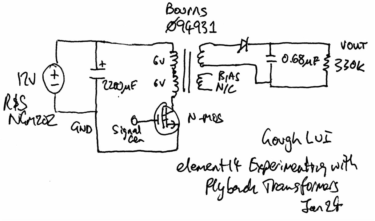
For this experiment, I chose the Bourns 094931 SP-E 20/6 Flyback Transformer. The reason for this is several fold – for one, I wanted to avoid high voltage in my experiments as even though my Keithley 2450 SMU could do 200V DC, I couldn’t confidently work with it and switch it quickly with my junk box parts. Remembering that the physics of transformers is (generally) reversible, the distinction in primary and secondary is merely by name. As long as the secondaries were rated at reasonable voltages that I could work with, I could drive them and expect the system to step-up the voltage to something bigger. The 094931 has two 6V/1.8A-rated secondaries, which could be wired in series so I could drive it nicely from 12V – a nice win.
Another reason for this choice is that generating high voltages from low voltages can be immensely useful. Things like cold-cathode tubes and Geiger counter tubes require high bias voltages, so to run these from batteries requires producing a high voltage from a low voltage. While it is possible to use boost converters and voltage multipliers to get there (depending on current requirements), the isolated nature of a flyback may have some safety benefits as well.
Nevertheless, this transformer claims a 19.75 : 2.75 : 1 : 1 ratio. As a result, I would expect, giving 12V to the two 6V windings in series, I would get 19.75 x 6V = 118.5V from the primary which is quite decent. I decided to keep things simple and left the bias winding open, but were I greedy, I could have series this with the primary to get a total of 22.5 : 1 ratio or an expected 135V.
Of course, the simple circuit needs some additional “helpers” – the first being a tanky primary side capacitor. This was mainly just out of concern that the wildly rapidly pulsating current may not play well with my wires and the power supply, even though I chose to use a very competent and fast Rohde & Schwarz NGM202 for this experiment. The second is a rectifying diode for the output, which I chose to use a classic 1N4004 (400V, 1A, 0.7V Silicon) – inexpensive, somewhat fast but perhaps not low-loss. For the capacitor to smooth the output voltage, I used an X2 safety rated capacitor, 0.68uF 250V AC-rated. Being a polyester film capacitor, usually these are pretty tolerant of a bit of overload. Of course, because I didn’t want to get zapped, there had to be a load to quickly discharge the capacitor once power was shut down, so I chose a 330kΩ 1/4W carbon film resistor from the junk box.
The switching element is classically an N-MOSFET and I have not deviated from this. Rummaging through my junk box, I found some Rds Test PCBs I had previously built with certain MOSFETs mounted on them. As a result, I pressed one back into service for this experiment – one containing an ST Microelectronics STP22NF03L (30V, 22A, 50mΩ). I do realise that my “addiction” to low-Rds MOSFETs is unhealthy when it comes to fast switching due to high gate charge/capacitance and reduced breakdown voltages, that is what I have to hand.
To drive this, I would simply use the onboard signal generator on the Rohde & Schwarz MXO4 Oscilloscope (review pending, coming soon). As such signal generators typically have a source impedance of 50Ω, this is not ideal for quickly changing the gate voltage, but it may still be a good enough drive (at least initially).
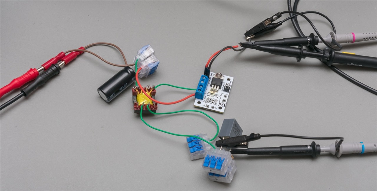
So far, so good, so let’s try to build this thing. Not being able to find my breadboard at this stage, but having my box of freshly delivered Ideal Gen II Lever Wire Connectors (thanks to element14’s Connect Magazine specials), I decided to opt for a build based on these solder-less connectors.
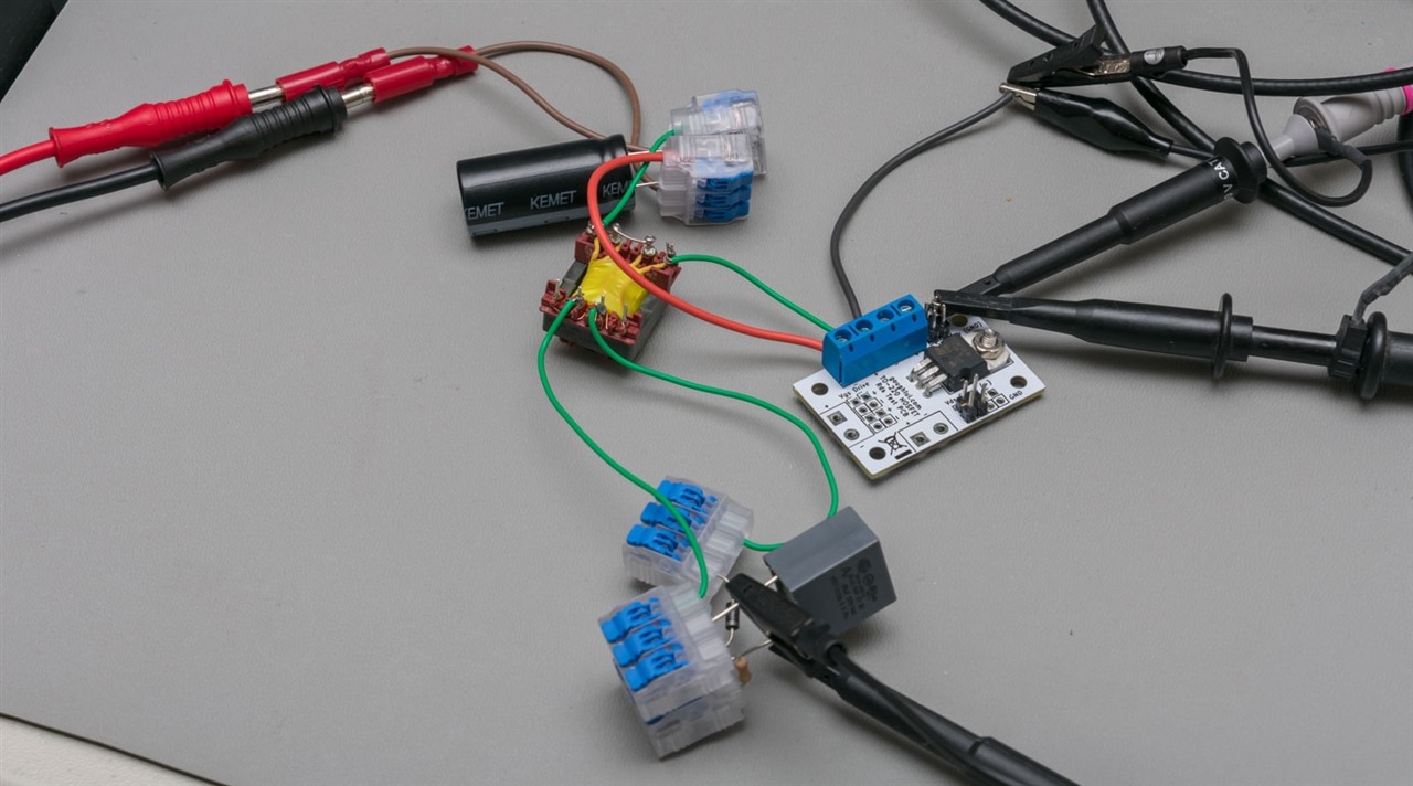
They’re like Wago connectors, just with the levers reversed … but it means for swift connections that can be broken at will and can handle some significant current. Consider this “air-wire” construction, quite literally. Solid core wire (in green) were soldered to the transformer terminals to ease connections to the terminal blocks.
Attempt #1: It Works … Sort-Of.
Setting the signal generator to 132kHz Square Wave, 10V drive with 5V offset (so as to swing between 0V and 10V to drive the gate “hard”) and 50% duty cycle (because it seemed a good value) … I didn’t expect it to work when I applied the power.
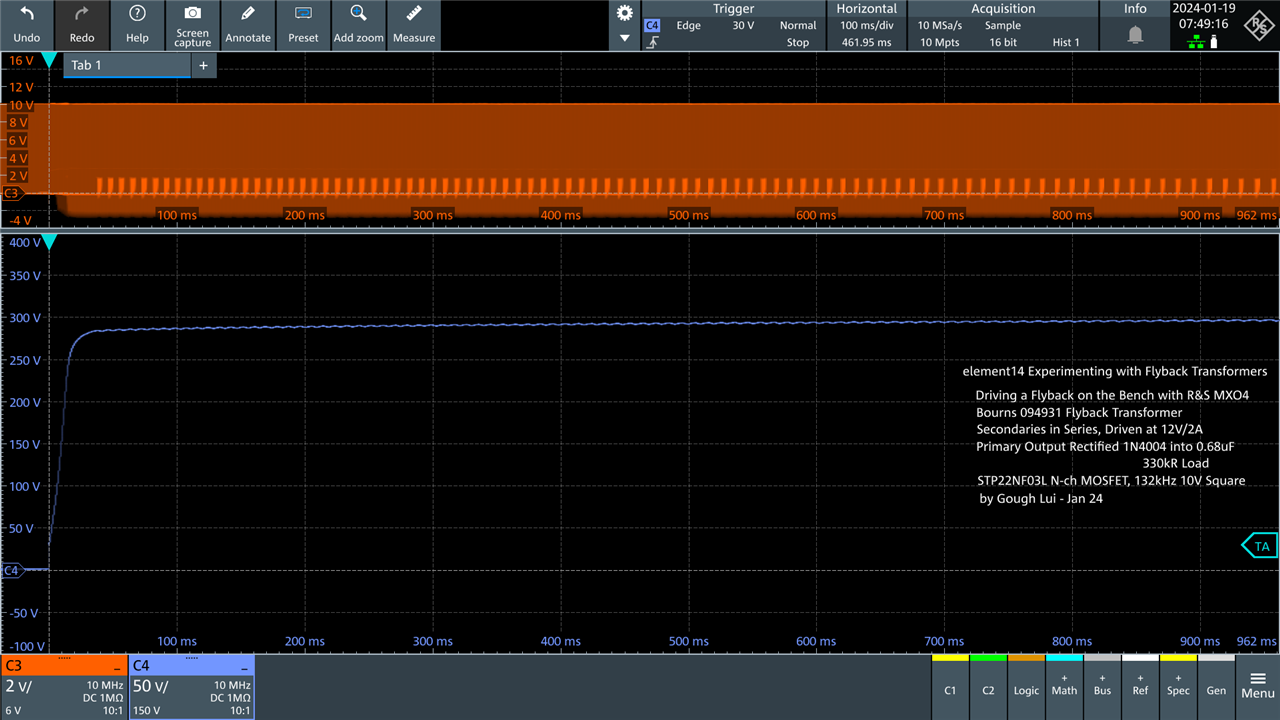
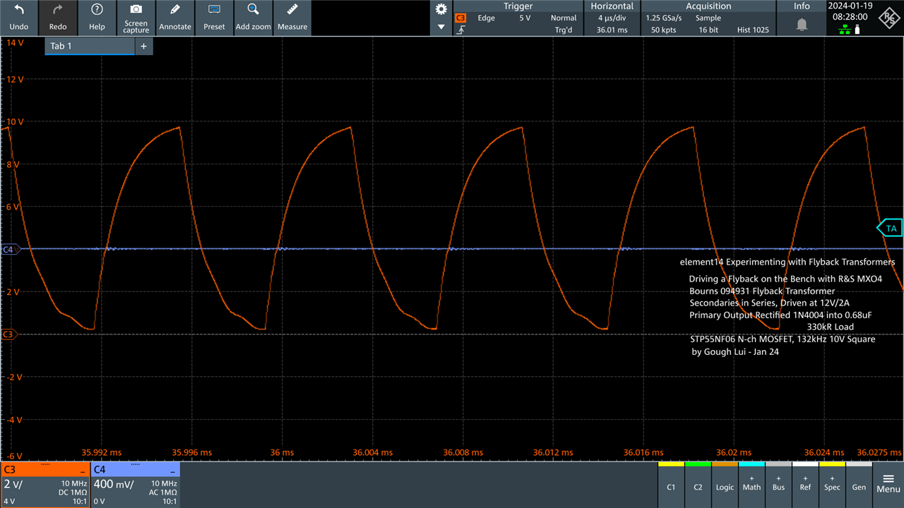
But it did. It created an output voltage just shy of 300V, more than twice what I was expecting. It also seemed to be a bit of a current hog – it was drawing about 1.6A from my supply which seemed a bit much. In these diagrams, C4 (Purple) is the flyback output voltage and C3 (orange) is the gate input voltage.
Overjoyed that something actually happened this time. I turned it off, set my scope up differently and powered it back up again.
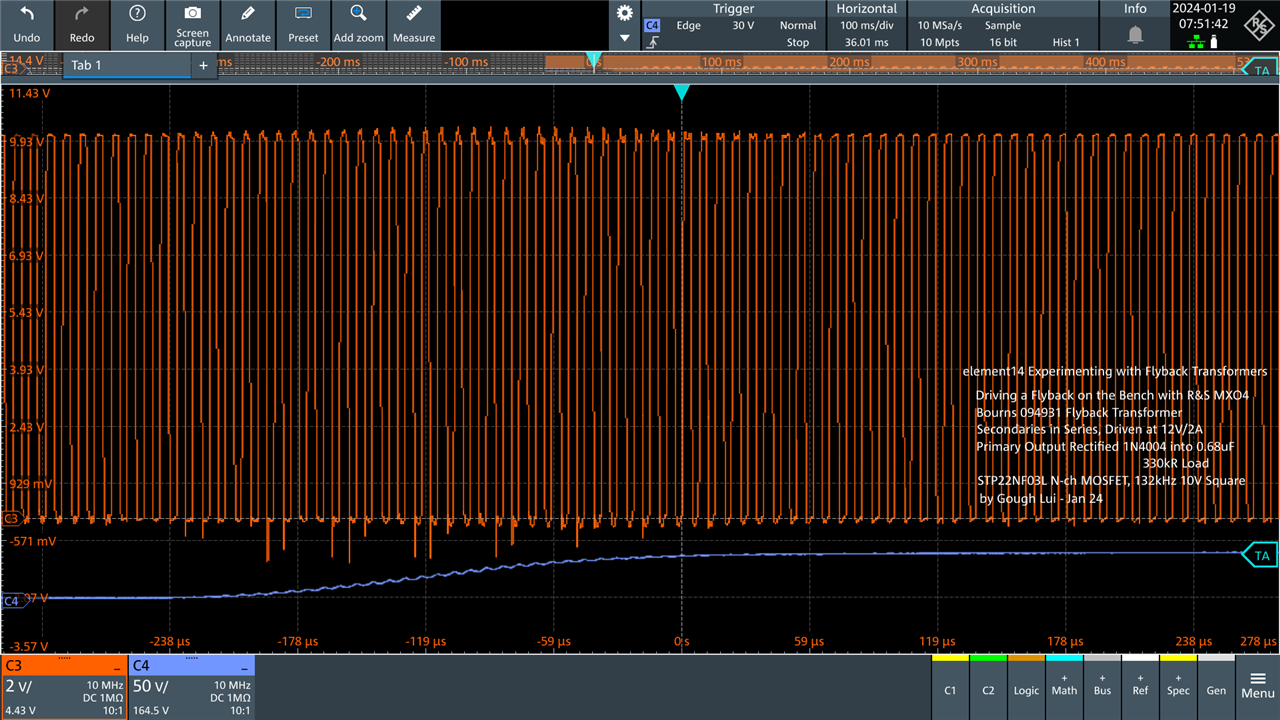
Using a lot of zoom, we can see how it starts up – the voltage does have “ripples” between each pulse, indicating that it is doing what a flyback does – charging the magnetic core through the primary when the MOSFET is turned on and dumping that into the secondary when the MOSFET is opened.
So why is the output voltage higher? I suspect it’s because of inductive kick or perhaps because there is some sort of ringing. But it’s perhaps a nice bonus.
But before I could celebrate and get some more results, it stopped working. Instead, now, it wasn’t showing any of its flyback behaviour and it seemed to be loading the supply a lot more.
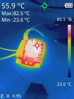
Without thinking, I decided to feel around to see if anything was hot and the MOSFET was literally burning. The tip of my index finger definitely felt it – this thermal image was taken a whole minute afterward. Remember in the last blog when I said I’d be licking my wounds … yeah. I wasn’t kidding. If you have a thermal camera … don’t use your fingers. Better yet, don’t use your fingers at all … or perhaps less valuable ones.
Attempt #2: I’m Not a Chef. Why Am I Cooking Chips?
Time to do a quick brainstorm … I’m one MOSFET down and I’ve got little clue as to why. Let’s take a few stabs in the dark:
- The STP22NF03L is a “logic-level” MOSFET (hence the L). This means it has a low-voltage threshold (1V) and its gate is quite sensitive. Perhaps I was pumping it a bit too quickly or too hard with the signal generator? But it is rated up to 15V (absolute maximum) so perhaps that’s not it.
- Perhaps my edges were too slow and it was dissipating too much power? But the ‘scope did show my edges were pretty sharp.
- Maybe the 30V Vds breakdown rating is not enough? I am operating 12V … so I’d expect perhaps 24V is enough in an ideal world, so maybe I’m onto something with this one. There’s probably some bounciness in the rails and my grounding was horrible before (as I discovered my gate signal was sharing a ground path with the current through the flyback … whoops!).
- Insufficient cooling – duh, I was relying on a piece of FR4 with two-sided 1-oz copper in a relatively small patch … but I wasn’t expecting much dissipation to begin with.
So I got out the desoldering tool, whipped off the dead MOSFET and chucked in an ST Microelectronics ST55NF06. This time, it’s 60V, 50A, 18mΩ rated with a normal threshold gate that can tolerate 20V absolute maximum. Surely, this uprated MOSFET (which I have a stack of thanks to a hamfest surplus clearance) would be up to the task! I also improved the grounding, providing a direct ground path to the MOSFET independent of the flyback’s ground path to avoid voltage differentials.
I put it into circuit, but then I decided to take off the supply to the flyback just to begin with.
Turns out the gate on this MOSFET is a big one as my signal generator is putting out shark-fins rather than square waves. [Insert expletive of choice].
While the MOSFET may be up to the task, the signal generator is not … and with this kind of slow turn on/off, I can expect only wonky results and perhaps even more dissipation than before.
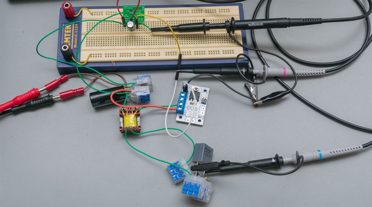
This is where I should be using a proper gate driver IC. I tried looking for my Infineon 1EDN8550B Gate Driver from a previous RoadTest but cannot locate the evaluation board. A second-best would probably be to use an opamp as a voltage follower and have that “buffer” the signal generator output and provide the bulk of the current. The problem? I don’t have many opamps on hand that can handle 10V+ and the ones that I do are slow with GBP of 1MHz and slew rates no more than about 5V/µs. The best I had was an OPA990 which I soldered onto a breakout and powered from the same 12V bus as the flyback itself …
… but this resulted in a more trapezoid waveform.
At least it looked somewhat nicer … even if it is slow. I guess I won’t have to be concerned about potential for dV/dT failures of MOSFETs with such a slow gentle waveform, but instead dissipation and linear-region operation is the concern instead.
After plugging in the flyback, the gate waveform now looks very strange indeed. At a duty cycle of 50%, I’m now getting 500V on the output – I wonder if this is because the capacitor itself is “leaking” enough to balance the voltage out or whether it’s the 1N4004 reaching its true limit (400V rated, likely with some headroom) and breaking down, but not passing enough energy to actually harm itself. This is a very suspicious number to arrive at.
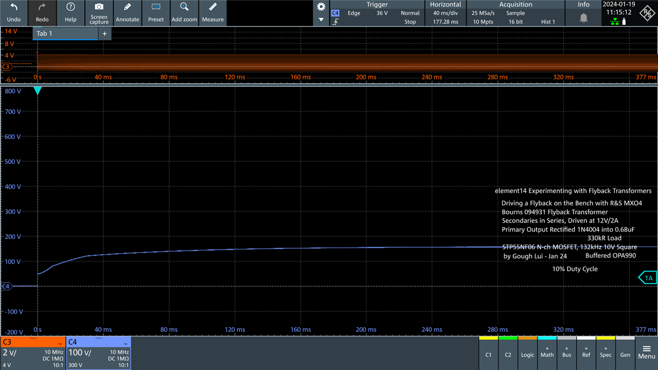
Reducing the duty cycle to 10% dropped the voltage to a more manageable 160V or so. As a result, it seems we have been able to show the use of duty cycle to control the transferred energy and thus, regulate the voltage (assuming you have some feedback and a controller that can modulate the duty cycle).
Not long after this … this MOSFET perished as well, as I was not taking care of the heat while gawking at the results and trying repeatedly to get meaningful oscilloscope captures.
Attempt #3: Still Getting More Than I Bargained For!
I’m not made of money but my junk box has more to give. This time, for better or for worse, I decided to see whether life would be easier with a different MOSFET. This time, I chose the International Rectifier IRFZ34E, a rather long-lived product with ratings of 60V/28A/42mΩ. I’m just hoping that this one might be a bit less of a gate capacitance issue.
To ensure its longevity, I caved and decided to use a USB fan, powered by a powerbank, to give a bit of forced convective cooling. It may be cheating, in a sense, but I need my results and time’s running out!
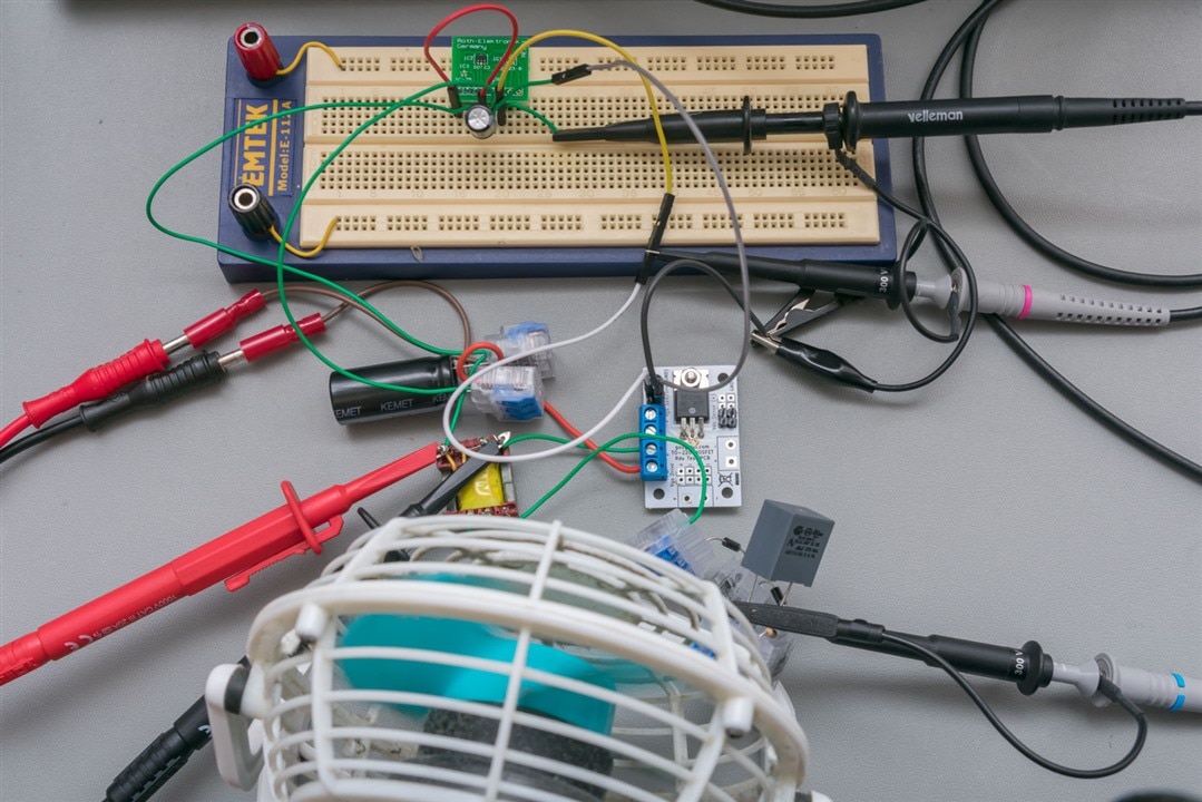
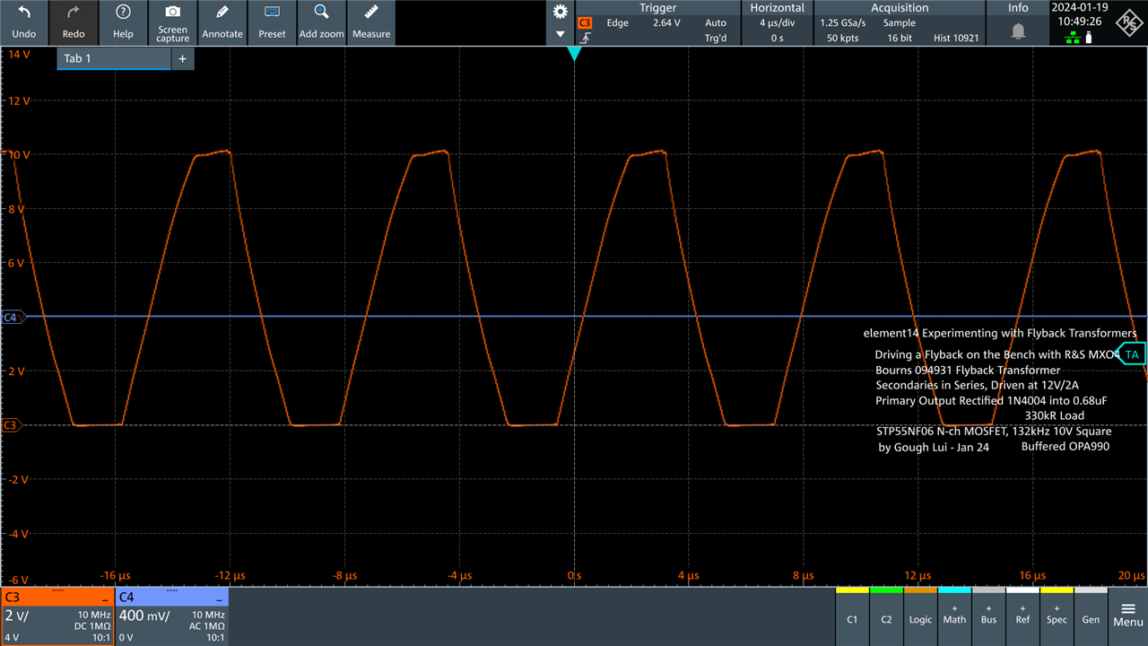
I’ve also added a high-voltage differential probe (HVP-70) to measure between the secondary windings (driven with 12V) to understand better what is happening at least with the voltage. I don’t have any current probes though. In the following diagrams, C4 (Purple) is the flyback output voltage, C3 (orange) is the gate input voltage and C2 (green) is the voltage across the flyback input winding.
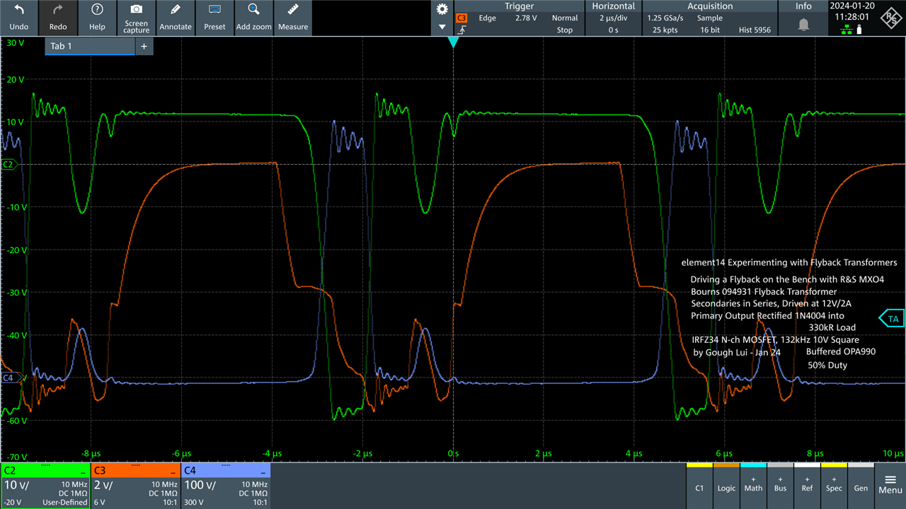
I removed the output capacitor to see how the circuit is really behaving. Looking at the flyback input voltage in green, we can see that flyback action is actually happening. The trigger point is when the MOSFET is turned on, and the coil is nicely charging at 12V. As the MOSFET turns off (somewhat delayed), the input coil drops negative and the output coil “flies” back to a much higher voltage – in this case, we’re seeing about 600V peak! Part of this is winding ratio, but the other may be some kind of resonance (with the ringing) and inductive “kick”, but I’m not entirely sure. This “flyback” action on the output coil only lasts a while until the field seemingly collapses and then the input coil voltage “flies up” again with a seemingly bigger ring before the cycle begins itself anew.
Looking at this, I am somewhat confused. I didn’t realise that during the flyback, the primary voltage would get so negative, even if briefly. I would expect the MOSFET’s body diode to conduct in about 100ns which I would have imagined would short it out if the coil developed a negative voltage. Considering this “peak” – if it were real, would have resulted in 1185V on the secondary by pure ratio – but perhaps the 330kΩ load dragged this down to the ~600V peak observed. The ringing is quite an interesting phenomenon – perhaps it’s affecting the ground enough that the MOSFET’s actually getting to the point of a partial turn-on during one of the rings. Maybe the faster edges in some cases were provoking more severe ringing, heating up and killing the MOSFETs quicker.
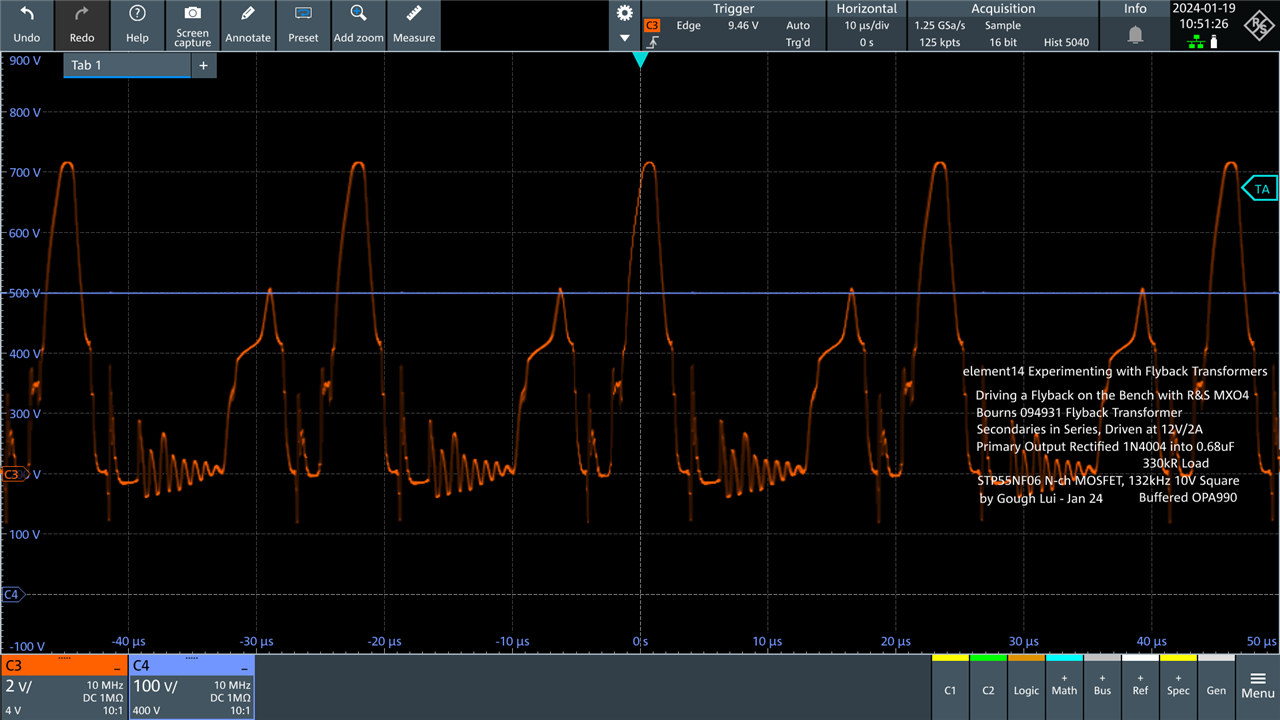
At this point, seeing the voltages are approaching 600V, I wondered if it’s the 1N4004 that’s letting me down. I decide to replace it with two 1N4004’s in series for a total of 800V to see if the output voltage would rise – it didn’t. I wonder if increasing the MOSFET’s Vds breakdown rating would help there or whether it’s something else entirely (perhaps the Q of the transformer itself).
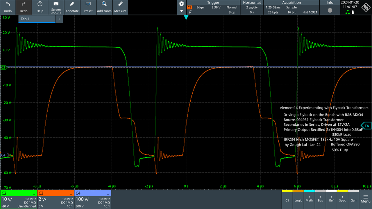
Here’s the same test with the output capacitor connected – the ringing is quite a bit cleaner to see and the nature of the ringing is different. Perhaps this is removing the secondary ringing from reflecting back into the primary.
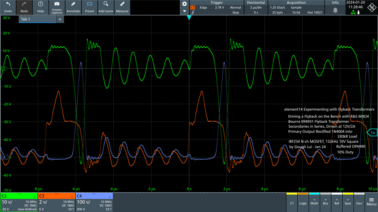
Dropping the duty cycle to 10% seems to show the ringing behaviour more clearly, with two different ringing frequencies observed. The voltage spike is more like 530V now, but for a shorter time, which when smoothed by a capacitor, results in a lower (average) voltage.
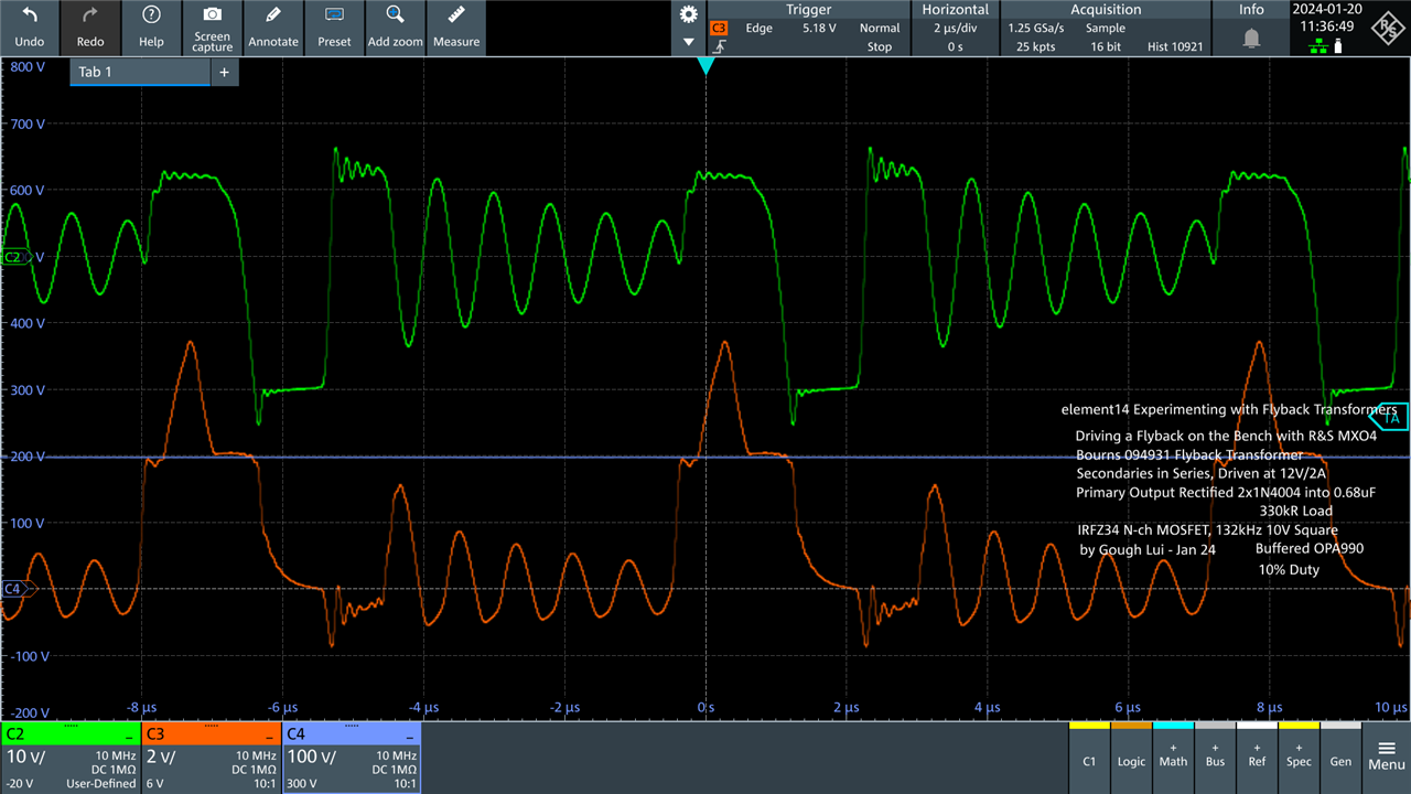
Here’s the same test with the capacitor plugged in. The waveform differs subtly when the output is smoothed – it seems less secondary ringing means less secondary ringing being inducted into other parts of the system.
What is the Fix? How to Make It Practical?
I think it should be quite obvious that most simple circuits are not practical circuits in real life. For one, such a circuit has ignored the need for regulation. In a practical use, the output voltage is usually regulated to a constant value even in the face of varying loads. In order to do this requires adjusting duty cycles or even skipping pulses under light loads (if energy efficiency is to be concerned). This is usually done with a flyback controller IC to automate the control aspects. Regulation would entail sensing the output voltage and feeding this back safely, which in traditional designs would rely on an optocoupler. In newer designs, there is the potential to use primary side sensing as an alternative (as the cheap Chinese USB power supplies seem to have used). Each has their own regulation benefits and complexity drawbacks, but it is important that isolation is maintained in this feedback system to ensure the isolation benefit of the flyback transformers can be fully realised.
Another issue that isn’t discussed is simply the EMI potential as many different frequencies are being generated in this circuit that can possibly be emitted along connecting wires and cause interference to other electronic devices. This is where the use of the common-mode choke can help, along with various design features to reduce the likelihood of emissions (e.g. bypass capacitors, snubbers and ferrite beads).
Of course, a big contributor to that (and the issues observed above) is the ringing itself. A proper way of dealing with the ringing would be to use a RCD snubber, as recommended in this Analog Devices Inc Technical Article and this Fairchild Application Note AN-4147. The use of a well-calculated resistor, capacitor and diode will allow for absorbing just the surge voltage in each cycle, while reducing energy losses. Unfortunately, this is beyond my current level of understanding and outside the time available for me to implement – but it’s nice to be aware of the proper way to solve the issue and the types of resonances that cause it.
Conclusion
My hubris led me back to starting at the bottom. Needless to say, the experience was a rather drawn-out one, knowing that most basic circuits never work reliably in practice. In this case, I observed flyback action and achieved much higher voltages than I expected. In the process of testing, I destroyed two MOSFETs likely because I let them overheat, likely bought about due to poor grounding, heavy ringing signals and poor edge transitions due to a lack of a proper gate driver (although an opamp was pressed into service, its slew rate was far from ideal as well). In doing so, I was able to identify shortcomings and understand the proper way forward, even if time doesn’t permit its implementation.
I suppose, in the end, while the whole series of blogs could be considered anti-climactic, it has been also mostly a success having achieved a majority of the aims I had set out to achieve in my proposal in such a limited time. While I don’t expect this to be award winning, compared to the efforts of other challengers, at least, I can say I gave it a red-hot go … quite literally. Now I’ll have to give my index finger some time to heal. Hot chips of the wrong sort …
Spoiler alert - the next blog, being the final blog, will summarise all of the findings thus far. There will be no new findings, so feel free to skip if you’ve followed along thus far, but it is mandatory for judging purposes so I will upload it later in the week once I have time to assemble it.
EDIT: Looks like there'll be a small surprise in the final blog. Small, being the key word.
Top Comments