In the first blog Introduction and Plan! - Experimenting with Magnetic Components, I gave a sneak peak about the plan to play around magnetics by devising a buck, flyback and designing a circuit with common mode choke to reduce noise at the power output. Here comes the proceedings:
The buck
Its by far the most common topology of power converters that we can find around us. The way it works is that when the MOSFET switch is ON, the current flows through the outer loop of circuit and starts charging the capacitor through inductor. The capacitor may not get fully charged(i.e., upto supply voltage) because of capacitors hesitation to charge instantly (there's this time constant ) and inductors attitude to limit charging current.
In the soon next instant(some microseconds), the MOSFET is switched off and since the current in an inductor cannot change suddenly, voltage is created across it and this is allowed to charge the capacitor. It now powers the load through the diode when the switch is turned off, maintaining the current output current throughout the switching cycle. This is the skeleton of the buck convertor stage and does not use any feedback or output regulation for varying load.
The unseen side in the above schematic is the main switching controller. It has to reliably switch at some tens of kHz frequency(atleast for this basic design). Since I wanted to experiment around and tune parameters on the fly, I thought of using IC555 in astable multivibrator mode for getting this action. The fun part in this is that by tweaking R1 and R2 (10K pots) the output signal frequency and duty cycle can be tuned.
f = 1/T = 1.44 / [(R1 + 2*R2)*C]
Duty Cycle = Ton/ [Ton + Toff]
= (R1 + R2) /(R1 + 2*R2) %
Here the tuning parameter is R1 and R2 just because it's far easier to find a variable resistor than a capacitor and also resistance has a strong correlation with the output frequency and duty cycle.
Breadboarding
The controller side, IC555 rig-up being pretty standard, I am using a TP2014 PMOS, IN4007 general purpose diode, RLB0914-102 1mH, 300mA radial inductor and the untold one, 100uF capacitor for this design.
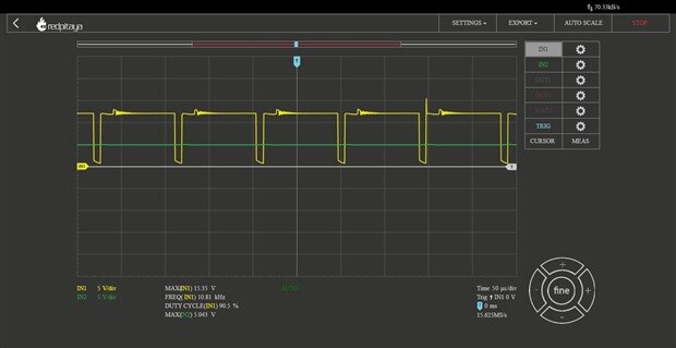
That's around 5V for a 12V input after switching tuning the frequency and at a duty cycle of 90.5% (yes, it's inverse. PMOS switching logic). To have the design more stable and get things tested, I moved on to a cladboard design.
Clad design, Layout and Soldering
The close enough performance is seen again with a cladboard circuit of the buck stage. The output voltage is always tuneable by adjusting the R1, R2 values of the IC 555 astable multivibrator thereby controlling the switching frequency of the bucking stage.
This is a plain buck stage design though and has terrible load regulation without any backsense or feedback of load current. But this does give a feel of bucking and the magnetics action behind it.
The Flyback
Flyback is just another power converter topology and what's special in it is that this is an isolated converter topology. The coupled inductor or so called flyback transformer is what magnetically bridges the input-output sections. This can work as both buck or boost based on the turns ratio of the flyback transformer.
In this design, I am using the HCTSM80102AAL part provided in the kit. It is 1:2 transformer and I am using the secondary side on the input and primary at the output to work for bucking. By not looking into the 2N7000 NMOS datasheet, I hooked up the circuit with this random NMOS which I had stocked by sampling from Microchip. The MOSFET CTRL pin is synced to the same IC555 multivibrator circuit(but keeping duty cycle <50% for bucking with the NMOS), here goes the circuit.
No output, no balsts -- but magic smoke (I was trying this circuit for the flyback with 2N222 BJT as a MOSFET driver)
My bad. The 12V input rail got shorted through the MOSFET pulling in all the current through it. More discussions on it here
I then changed the MOSFET driving section and put back direct control of NMOS Gate from the IC555 multivibrator. This time the IRF540 power MOSFET(same as in the above flyback circuit)
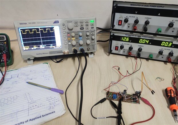
(PS: no wonder, these test gears are university property. And yes, the bench supply has 0.6V offset incase you're wondering about the odd voltage value shown)
On testing, this does give a tolerable stable output voltage, but again, load regulation isn't great. Here is a clip of output voltages on loading:
> Output adjusted to 2V at no-load
> 852mV at 1K load
> 320mV at 100R load
I am working on adding a feedback network to the same buck stage for making the system regulatable towards output loading and also the addition of protection circuitry for surges and short circuits. It was a good learning and making experience working around magnetics and trying out different topologies. I feel there is way more to explore, experience and workaround these power converter topologies. Would love to get some suggestions on these 
| Links and References |
|---|
| 555 Oscillator Tutorial - The Astable Multivibrator (electronics-tutorials.ws) |
| Flyback Topology and Specs by TI: https://www.ti.com/lit/an/snva716/snva716.pdf |
| Basic Linear Design Seminar - Chapter 9 (analog.com) |
| Power Topologies Quick Reference Guide by TI: https://www.ti.com/lit/ug/slyu032/slyu032.pdf |
| Flyback Converter : Design, Working, Calculations & Its Applications (elprocus.com) |


