element14 Community
element14 Community
    Register Log In
  • Site
  • Search
  • Log In Register
  • Community Hub
    Community Hub
    • What's New on element14
    • Feedback and Support
    • Benefits of Membership
    • Personal Blogs
    • Members Area
    • Achievement Levels
  • Learn
    Learn
    • Ask an Expert
    • eBooks
    • element14 presents
    • Learning Center
    • Tech Spotlight
    • STEM Academy
    • Webinars, Training and Events
    • Learning Groups
  • Technologies
    Technologies
    • 3D Printing
    • FPGA
    • Industrial Automation
    • Internet of Things
    • Power & Energy
    • Sensors
    • Technology Groups
  • Challenges & Projects
    Challenges & Projects
    • Design Challenges
    • element14 presents Projects
    • Project14
    • Arduino Projects
    • Raspberry Pi Projects
    • Project Groups
  • Products
    Products
    • Arduino
    • Avnet Boards Community
    • Dev Tools
    • Manufacturers
    • Multicomp Pro
    • Product Groups
    • Raspberry Pi
    • RoadTests & Reviews
  • Store
    Store
    • Visit Your Store
    • Choose another store...
      • Europe
      •  Austria (German)
      •  Belgium (Dutch, French)
      •  Bulgaria (Bulgarian)
      •  Czech Republic (Czech)
      •  Denmark (Danish)
      •  Estonia (Estonian)
      •  Finland (Finnish)
      •  France (French)
      •  Germany (German)
      •  Hungary (Hungarian)
      •  Ireland
      •  Israel
      •  Italy (Italian)
      •  Latvia (Latvian)
      •  
      •  Lithuania (Lithuanian)
      •  Netherlands (Dutch)
      •  Norway (Norwegian)
      •  Poland (Polish)
      •  Portugal (Portuguese)
      •  Romania (Romanian)
      •  Russia (Russian)
      •  Slovakia (Slovak)
      •  Slovenia (Slovenian)
      •  Spain (Spanish)
      •  Sweden (Swedish)
      •  Switzerland(German, French)
      •  Turkey (Turkish)
      •  United Kingdom
      • Asia Pacific
      •  Australia
      •  China
      •  Hong Kong
      •  India
      •  Korea (Korean)
      •  Malaysia
      •  New Zealand
      •  Philippines
      •  Singapore
      •  Taiwan
      •  Thailand (Thai)
      • Americas
      •  Brazil (Portuguese)
      •  Canada
      •  Mexico (Spanish)
      •  United States
      Can't find the country/region you're looking for? Visit our export site or find a local distributor.
  • Translate
  • Profile
  • Settings
Experimenting with Magnetic Components
  • Challenges & Projects
  • Design Challenges
  • Experimenting with Magnetic Components
  • More
  • Cancel
Experimenting with Magnetic Components
Blog Test GaN Quick Mobile Charger Different CMC #2 The Uncompleted Experiment Report
  • Blog
  • Forum
  • Documents
  • Files
  • Mentions
  • Sub-Groups
  • Tags
  • More
  • Cancel
  • New
  • Share
  • More
  • Cancel
Group Actions
  • Group RSS
  • More
  • Cancel
Engagement
  • Author Author: fyaocn
  • Date Created: 15 Nov 2021 3:43 PM Date Created
  • Views 1159 views
  • Likes 5 likes
  • Comments 0 comments
Related
Recommended

Test GaN Quick Mobile Charger Different CMC #2 The Uncompleted Experiment Report

fyaocn
fyaocn
15 Nov 2021

    • 1 CMC  and Inductor in GaN Quick Charger
      • 1.1 The GaN Charger
      • 1.2 Common Mode Choke in the GaN charger
    • 2 The Parts and Circuits
      • 2.1 The part of CMC
      • 2.2 Circuit
    • 3 Performance
      • 3.1 Performance of original CMC
      • 3.2 Replacement of new CMC
    • 4  Summary

1 CMC  and Inductor in GaN Quick Charger

1.1 The GaN Charger

Suddenly, GaN charger becomes optimal choice for mobile. It is compact and super fast in charging. It is claimed that fast charge do no harm to mobile battery. At least for now, there is no obvious damage.

GaN Charger is fairly compact in size and intelligent charging with large current flow up to 3.25A. But the charger need mobile to support the quick charging protocol or it is just one normal charger.

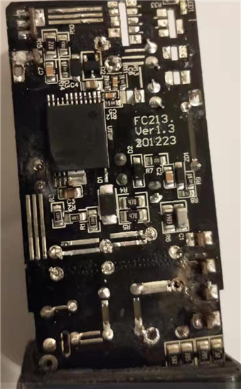
There are 3 output ports, two for quick charge and one for normal charging. After breakdown, three port are vertical on the base PCB board, each with  one smart Control chip.

Gallium nitride has a 3.4 eV bandgap, compared to silicon’s 1.12 eV bandgap. Gallium nitride’s wider bandgap means it can sustain higher voltages and higher temperatures than silicon.  Fast DC switch frequency for GaN is why  GaN can be made so small.


It is realy interesting to find out how the chip works, since there have been some cheating circuit to make this GaN charger one adjustable DC power.

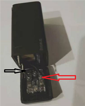
First, cut from one end with hand saw carefully since it is hot-welded without any screw.

image

Take out the fully copper covered PCB. Higher DC power frequency means more challenges on EMC and heat dissipation. With natural cooling, silicon-gel plays important roles.


imageimageimage

I have remove every parts with hot wind gun to study the circuit. I need to put them back for this experiment.

image

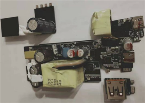
This is daughter board for fast charging control, with SW3518 from Ismartware, refer to http://www.ismartware.com/

Max power delivery PD for 45W with 18W for normal charging port.

image


1.2 Common Mode Choke in the GaN charger

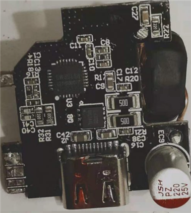
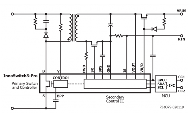
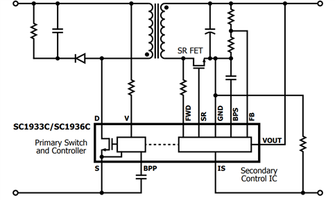
Power conversion part from AC to DC is PI SC1933, unfortunately, this is off-book from the official web. I have checked and assumed that new innoswitch3-pro series is new brand. refer to https://www.powerint.cn/products/innoswitch/innoswitch3-pro for more detail introduction. This is one GaN power delivery control chip integrated Power electronics and microchip to control with I2C. It takes more time, I can find how the I2C work with analyser, that would be perfect to make one smart DC Power bench with this retro-GaN charger. Here is the application diagram for PI Innoswith3-pro.

image


2 The Parts and Circuits

2.1 The part of CMC

Here is the type of Choke, Inductor and CMC as listed. Except that Item 8 is missing.
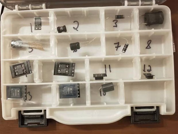
image

Item 9-12,

  imageimage


2.2 Circuit

Here is the circuit to be used , the GaN charger main board.

This is the proposed circuit for PI SC1933, similar to inno-switch3-pro,

image

typical design for notebook power shall be,

image

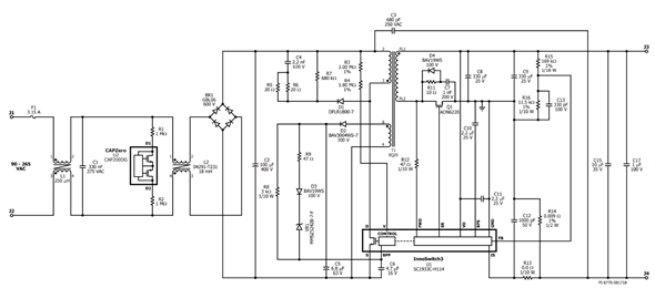
we can see there are two stage CMC used. But this circuit uses only one CMC.


3 Performance

3.1 Performance of original CMC

Unfortunately, during the experiment, the secondary winding of pulse transformer was short-circuited by probe of oscilloscope, the PCB is damaged.

image

This could have been avoided if test point was set in advanced in compact commercial products.


3.2 Replacement of new CMC

The experiment on CMC is not completed. I shall experiment this component in platform much better like Rohm SiC MOSFET"P02SCT3040KR-EVK-001

image

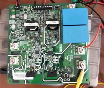
That is half bridge evaluation board, need peripherals circuit to make experiments.


4  Summary

Proper selection of CMC can reduce the EMI, balancing the performance and cost is common in mass production. In this GaN charger, only one stage of CMC is used just before pulse transformer with primary voltage of AC 220V.

I have planned to experiment this GaN charger with CMC. Then programming the PI SC1933 into one GaN DC power bank in arduino. I shall revise the plan and make further effort on how to continue the previous plan.

  • Sign in to reply
element14 Community

element14 is the first online community specifically for engineers. Connect with your peers and get expert answers to your questions.

  • Members
  • Learn
  • Technologies
  • Challenges & Projects
  • Products
  • Store
  • About Us
  • Feedback & Support
  • FAQs
  • Terms of Use
  • Privacy Policy
  • Legal and Copyright Notices
  • Sitemap
  • Cookies

An Avnet Company © 2025 Premier Farnell Limited. All Rights Reserved.

Premier Farnell Ltd, registered in England and Wales (no 00876412), registered office: Farnell House, Forge Lane, Leeds LS12 2NE.

ICP 备案号 10220084.

Follow element14

  • X
  • Facebook
  • linkedin
  • YouTube