PMOD ALS [Ambient Light Sensor]

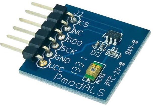
The Pmod ALS is a sophisticated peripheral that converts ambient light into digital signals that an FPGA (Field-Programmable Gate Array) can process. It consists of two main components :
1. Vishay TEMT6000X01

The TEMT6000X01 is a surface-mount phototransistor, housed in a tiny 1206 package (approximately 4mm x 2mm x 1mm). It's designed to detect visible light, much like the human eye, and its peak sensitivity is at a wavelength of 570 nanometers, which corresponds to green light. This means it's most responsive to green light and slightly less sensitive to other colors in the visible spectrum. The sensor's output is an analog current – more light, more current. A key parameter is its Collector-Emitter Breakdown Voltage (VCEO), which is the maximum voltage that can be applied between the collector and emitter pins without damaging the sensor. For the TEMT6000X01, this is 6V. Another crucial specification is the Collector Dark Current (ICEO), which is the small leakage current that flows through the sensor even in complete darkness. Typically, this is very low, around 50 nanoamperes (nA) or less. The photocurrent, which is the current generated in response to light, is typically around 10µA at 3.5lx and 50µA at 100lx under CIE illuminant A and a VCE of 5V. This effectively describes the sensor's sensitivity. The angle of half sensitivity is ±60 degrees, meaning the sensor's output is halved when light enters at a 60-degree angle compared to direct incidence. The spectral bandwidth ranges from 440nm to 800nm, covering a significant portion of the visible light spectrum. The sensor operates within a temperature range of -40°C to +100°C.
2. Texas Instruments ADC081S021
The Texas Instruments ADC081S021 is a small, low-power, 8-bit analog-to-digital converter (ADC) designed for single-channel applications. Think of it as a digital "translator" that takes an analog voltage (like the one produced by the TEMT6000X01 light sensor) and converts it into an equivalent 8-bit digital number. This ADC utilizes the successive approximation register (SAR) architecture, which is a common and efficient method for performing analog-to-digital conversions. It operates with a single power supply ranging from 2.7V to 5.25V, making it suitable for various applications and compatible with common microcontroller voltage levels. It has a serial interface, specifically designed to be compatible with standards like SPI, QSPI, and MICROWIRE, simplifying communication with microcontrollers.

One of its strengths is its flexibility in sampling rate, ranging from 50 ksps (kilo-samples per second) to 200 ksps. This means it can take anywhere from 50,000 to 200,000 samples of the analog voltage every second, offering adaptable performance for different applications. Accuracy is crucial in any ADC, and the ADC081S021 boasts decent linearity. Differential Nonlinearity (DNL), which measures the variation between the actual step sizes of the ADC's output and the ideal step size of 1 Least Significant Bit (LSB), is typically ±0.2 LSB. Integral Nonlinearity (INL), representing the maximum deviation of the ADC's transfer function from a straight line, is also around ±0.3 LSB. These specifications ensure the ADC provides a reasonably accurate digital representation of the analog input.
In terms of noise performance, the ADC081S021 has a typical Signal-to-Noise Ratio (SNR) of 49.6dB. This indicates the strength of the desired signal (the converted light level) compared to unwanted noise. A higher SNR generally means a cleaner and more accurate conversion. The ADC has a power-saving feature: a shutdown mode. When not actively converting, it can be placed in this mode to minimize power consumption, drawing as little as 2.6µW. The ADC081S021 comes in compact packaging options like SOT-23 and WSON, minimizing its physical footprint. It's specified for operation across a broad temperature range (-40°C to 85°C), making it suitable for use in various environments. Some key absolute maximum ratings, which must never be exceeded, include a maximum analog input voltage of 6.5V and a maximum allowable junction temperature of 150°C.
Now, let's explore how this remarkable system works and how it interfaces with our digital design!
Working
At the heart of the Pmod ALS is the Vishay TEMT6000X01 ambient light sensor. Think of this sensor as a highly sensitive electronic eye – it's a phototransistor that exhibits variable conductivity based on incident light.

When photons strike the semiconductor material, they create electron-hole pairs, increasing the device's conductivity proportionally to the light intensity. This phenomenon results in a current flow through a precision resistor, generating an analog voltage signal that represents the ambient light level. Imagine this as the first stage of our signal processing chain, where physical light energy is transformed into an electrical quantity.
However, FPGAs operate in the digital domain, working with discrete logic levels and binary values. They can't directly interpret continuous analog signals. This is where the Texas Instruments ADC081S021 analog-to-digital converter (ADC) becomes crucial. The ADC bridges the analog and digital worlds, converting the continuous voltage levels into digital codes that our FPGA design can process using standard digital logic.

The ADC performs this conversion through a sophisticated process that can be synchronized with our FPGA's clock domain. First, it captures the analog voltage in a sample-and-hold circuit, effectively freezing the voltage level for conversion. This sampling is crucial for maintaining signal integrity and can be precisely timed using the FPGA's clock management resources. The ADC then employs a successive approximation register (SAR) architecture, which uses an internal digital-to-analog converter (DAC) and comparator to perform binary search quantization. Since this is an 8-bit ADC, it divides the input voltage range into 256 discrete levels, providing a resolution suitable for most ambient light sensing applications.
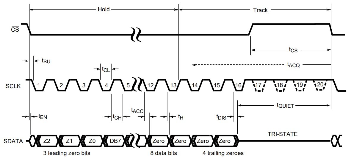
The 8-bit digital value from the ADC is made available to the FPGA through the Serial Peripheral Interface (SPI). The Pmod ALS is typically configured as an SPI slave device. The microcontroller, acting as the SPI master, initiates communication by pulling the Chip Select (CS) line low. It then provides the clock signal (SCLK) to synchronize data transfer. The ADC sends the converted data to the microcontroller on the Master In Slave Out (MISO or SDO) line. The data is transmitted serially, one bit at a time, synchronized with the SCLK. The ADC081S021 outputs the 8-bit data with leading and trailing zeros as shown below.

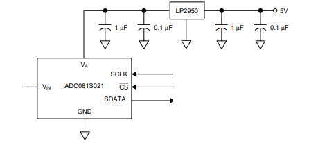
Block Diagram

References
1. https://digilent.com/reference/pmod/pmodals/reference-manual
2. https://www.ti.com/lit/ds/symlink/adc081s021.pdf
3. https://www.vishay.com/docs/81579/temt6000.pdf
