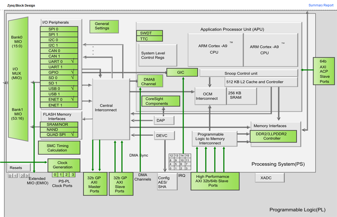
Many computer architectures contains more than a processor, consequently, the developer must change the programming perspective in order to use each available resource in the platform. This time, the XC7Z020 SoC has a Dual-core ARM Cortex-A9 in the Hard Processor system. By default, the platform designed uses the UART0 for communications, the GPIO insterface is enabled and the Ethernet port for future usage is connected. The UART is configured as 115200@8N1, the most common configuration with stable features for communication between the Soc and the PC.
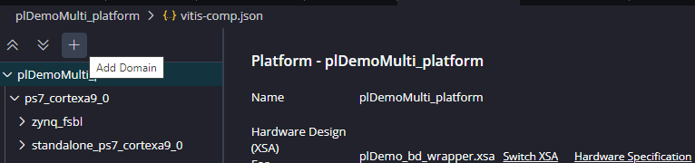
When the plartform is created in Vitis, only the CPU0 has a domain for the bare-metal software developing. This means that the CPU1 is stuck since there are no instructions for execution. To solve this, the platform must have a new Domain with the CPU1 as processor. To do, it is necessary Add Domain in the vitis-comp.json file, located on the platform settings. According to the block diagram created on the Vivado project, the objective is list each processor available in the system, if the developer includes a Microblaze core, this core should be accesible when the platform project is created or modified. All information is available in the exported XSA file.
| {gallery}Platform Architecture |
|---|
|
Add Domain: Create a domain for each processor to use. |
|
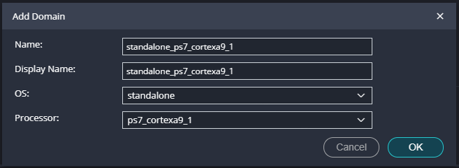
Domain Configuration: Configure the domain for the processor to add in the project |
|
Domain Tree: All the processor must have its description and configuration |
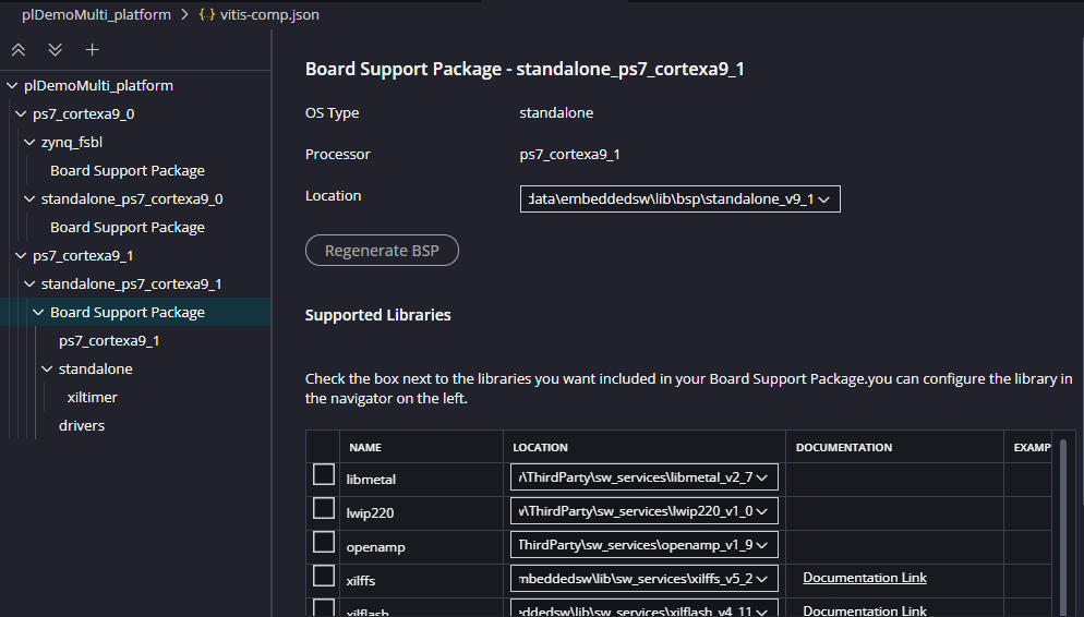
Only the CPU0 has the First Stage Boot Loader (fsbl) since the CPU0 has the highest priority in access and execution. Once the platform is configured and all the processors are reached by the project, the developer is able to create an application for each domain specified. For this test, an additional modification must be made in order to separate the access to the memory. The proposed segmentation is shown below,
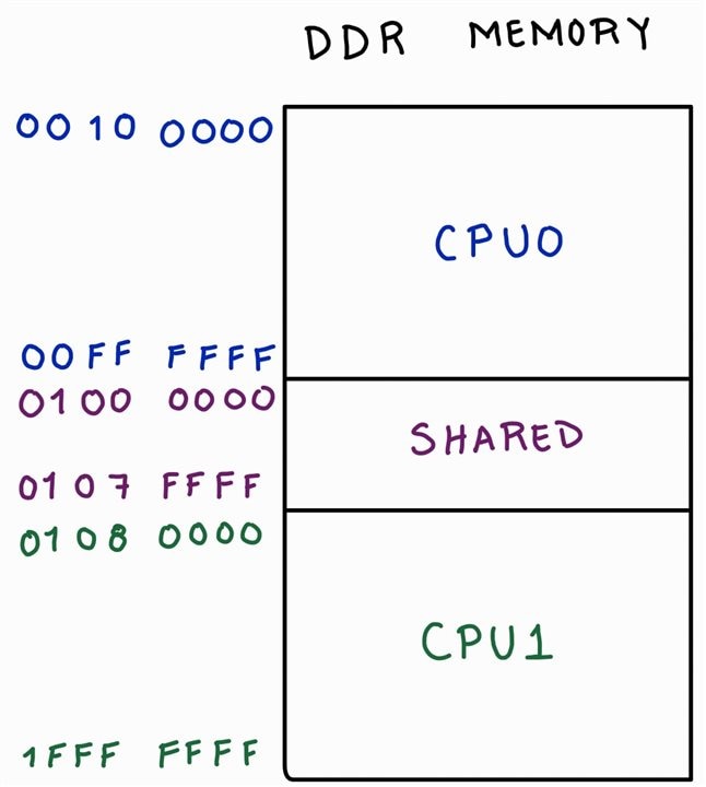
Here, the CPU0 will have the access to the addresses 0x00100000 to 0x00FFFFFF for the data management. On the other hand, the addresses 0x01080000 to 0x1FFFFFFF are reserved for the CPU1. Finally, the addresses 0x01000000 to 0x0107FFFF are reserved for data sharing between the processors. This is a proposal for the DDR memory segmentation, there will not data collision since all the common addresses has a controlled access internally. Now, the code implemented is the same as in the last blog for the CPU0, but with some modifications to share data and verify that the information is received by the processor CPU1.
//CPU0 code
#include <stdio.h>
#include "platform.h"
#include "xil_printf.h"
#include "xparameters.h"
#include "xil_io.h"
#include "xil_mmu.h"

#define ARM1_BASEADDR_REG 0xFFFFFFF0
#define ARM1_BASECODE   0x10080000

int main()
{
    init_platform();

    uint32_t btnIn;
    uint32_t ledState;

    volatile uint32_t *x = (uint32_t*)0x10000000;

    Xil_Out32(ARM1_BASEADDR_REG, ARM1_BASECODE);
    dmb();
    __asm__("sev");

    while(1){
        ledState = Xil_In32(XPAR_AXI_GPIO_0_BASEADDR);
        btnIn = Xil_In32(XPAR_AXI_GPIO_0_BASEADDR + 8);
        *x = btnIn;
        if(btnIn & 0x08){
            ledState &= ~0x07;
            ledState |= (btnIn & 0x07);
        }else{
            ledState &= ~0x38;
            ledState |= (btnIn & 0x07) << 3;
        }
        Xil_Out32(XPAR_AXI_GPIO_0_BASEADDR, ledState);
    }
    return 0;
}
//CPU1 code
#include <stdio.h>
#include "platform.h"
#include "xil_printf.h"
#include "PWMGen.h"
#include "sleep.h"
#include "xil_mmu.h"
int main()
{
init_platform();
volatile uint32_t *x = (uint32_t*)0x10000000;
uint32_t period = 10000;
float dc = 0.2;
while(1){
if(*x & 0x08){
if(*x & 0x04){
period += 1000;
}else{
period -= 1000;
}
}else if(*x & 0x02){
if(*x & 0x01){
dc += .1;
}else{
dc -= .1;
}
dc = (dc - 1.0 > 0.0)? 1.0: (dc < 0.0)? 0.0: dc;
}
DemoFrequency(0x43C00000, period);
DemoDuty(0x43C00000, dc);
sleep(1);
}
return 0;
}
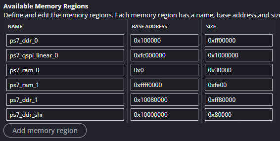
In terms of debugging, the ARM1_BASExxx are not necessary, but for production approaches, the coding and correct memory segmentation are required to execute both codes from the SD card. In order to guarantee the correct code loading, the CPU1 must be initialised from the CPU0. Remember! The CPU0 manages the resources from the fsbl to the final code execution. Consequently, the code base must be written to address 0xFFFFFFF0, this in accordance with the official documentation. The mentioned address must be the same address as the mentioned the in memory regions of each project. In addition to that, both projects must have the same specified memory regions to avoid collisions or access violations.
As shown in the figure above, this have the same memory segmentation is proposed for each DDR address. Once the application projects have been validated, they must be integrated into a system project as a whole. This allows the integration of both projects with a shared memory region to avoid access issues and to manage some tasks on one processor and others on the second processor.
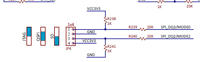
For the boot image generation, the developer must build the project using both code projects for each processor and ensure that all the required files(fsbl.elf,wrapper .bit file, and each elf file for the codes) are included in the project. This will generate a BOOT.bin file that needs to be written to a FAT32 formatted SD memory card to insert into the board and watch the magic happen. Remember! the JP4 must be configured for SD boot.