element14 Community
element14 Community
    Register Log In
  • Site
  • Search
  • Log In Register
  • Community Hub
    Community Hub
    • What's New on element14
    • Feedback and Support
    • Benefits of Membership
    • Personal Blogs
    • Members Area
    • Achievement Levels
  • Learn
    Learn
    • Ask an Expert
    • eBooks
    • element14 presents
    • Learning Center
    • Tech Spotlight
    • STEM Academy
    • Webinars, Training and Events
    • Learning Groups
  • Technologies
    Technologies
    • 3D Printing
    • FPGA
    • Industrial Automation
    • Internet of Things
    • Power & Energy
    • Sensors
    • Technology Groups
  • Challenges & Projects
    Challenges & Projects
    • Design Challenges
    • element14 presents Projects
    • Project14
    • Arduino Projects
    • Raspberry Pi Projects
    • Project Groups
  • Products
    Products
    • Arduino
    • Avnet & Tria Boards Community
    • Dev Tools
    • Manufacturers
    • Multicomp Pro
    • Product Groups
    • Raspberry Pi
    • RoadTests & Reviews
  • About Us
  • Store
    Store
    • Visit Your Store
    • Choose another store...
      • Europe
      •  Austria (German)
      •  Belgium (Dutch, French)
      •  Bulgaria (Bulgarian)
      •  Czech Republic (Czech)
      •  Denmark (Danish)
      •  Estonia (Estonian)
      •  Finland (Finnish)
      •  France (French)
      •  Germany (German)
      •  Hungary (Hungarian)
      •  Ireland
      •  Israel
      •  Italy (Italian)
      •  Latvia (Latvian)
      •  
      •  Lithuania (Lithuanian)
      •  Netherlands (Dutch)
      •  Norway (Norwegian)
      •  Poland (Polish)
      •  Portugal (Portuguese)
      •  Romania (Romanian)
      •  Russia (Russian)
      •  Slovakia (Slovak)
      •  Slovenia (Slovenian)
      •  Spain (Spanish)
      •  Sweden (Swedish)
      •  Switzerland(German, French)
      •  Turkey (Turkish)
      •  United Kingdom
      • Asia Pacific
      •  Australia
      •  China
      •  Hong Kong
      •  India
      • Japan
      •  Korea (Korean)
      •  Malaysia
      •  New Zealand
      •  Philippines
      •  Singapore
      •  Taiwan
      •  Thailand (Thai)
      • Vietnam
      • Americas
      •  Brazil (Portuguese)
      •  Canada
      •  Mexico (Spanish)
      •  United States
      Can't find the country/region you're looking for? Visit our export site or find a local distributor.
  • Translate
  • Profile
  • Settings
In the Air Design Challenge
  • Challenges & Projects
  • Design Challenges
  • In the Air Design Challenge
  • More
  • Cancel
In the Air Design Challenge
Blog In The Air: Episode 5 - PCB Design
  • Blog
  • Forum
  • Documents
  • Polls
  • Files
  • Events
  • Mentions
  • Sub-Groups
  • Tags
  • More
  • Cancel
  • New
  • Share
  • More
  • Cancel
Group Actions
  • Group RSS
  • More
  • Cancel
Engagement
  • Author Author: michaelwylie
  • Date Created: 2 Dec 2014 8:39 AM Date Created
  • Views 2990 views
  • Likes 4 likes
  • Comments 31 comments
  • iot_particle_counter
  • in_the_air
Related
Recommended

In The Air: Episode 5 - PCB Design

michaelwylie
michaelwylie
2 Dec 2014

Update

A Riddle: How many times in three weeks can a 1 year old child catch sick? The correct answer seems to be 3 times ...


Previous Posts

In The Air: Epidose 1: Introduction

In The Air: Episode 2 - Preparing for Surface Mount Work

In The Air: Episode 3 - Surface Mount Beginnings

In The Air: Episode 4 - Inductors


Introduction

I have finished my Booster Pack design. Figure 1 shows the top and bottom layers. Note, I am an Altium user so the display of the board layers may be unfamiliar to you if you are an Eagle user. If you are familiar with TI's Booster Packs, you'll recognize the characteristic 20 pin headers on opposing sides of the board. In my last post I discussed choosing inductors for filtering/decoupling grounds and power supplies. Accordingly, we will discuss the layout of those inductors and separating grounds for quiet sensor performance in this post.


Figure 1: Bottom (left) and top (right) layers for my Booster Pack design.
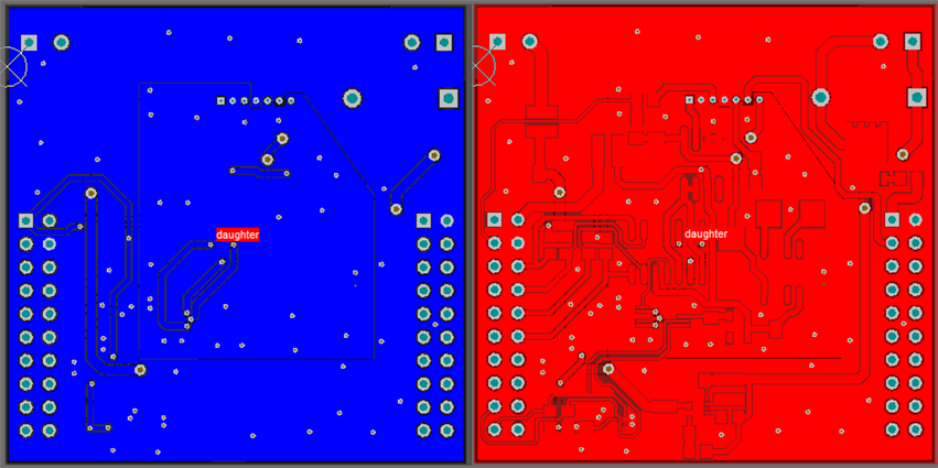
image


Connecting Grounds

The general approach I have adopted is shown in Figure 3. The signal ground is like an island surrounded by the power ground, and the only way to get to the signal ground is through an inductor. The connector is on the boundary between the two grounds because the sensor requires both power and signal ground. I've created an annotated version of the board layout of Figure 1 and produced it in Figure 4. I have labelled the sensor interface, signal ground, and power ground. The power ground is directly connected to the ground of the C3200 through the Booster Pack header connections, and the signal ground is connected to the power ground through the aforementioned inductor.


image

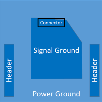
Figure 3: Basic idea of the Particle Counter Booster Pack.


image

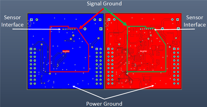
Figure 4: Annotated Figure 1 showing the sensor interface, signal ground, and power ground.


In Figure 5 I've zoomed in on the board so the signal ground is more visible, and the ground connecting inductor can be seen in the lower left (L2). You can't see the pads from the component because I used Seeedstudio Fusion for my PCBs, and Seeed Studio's design rules don't use a thermal relief pad connection by default. I'm not sure why, but that's the way it loaded. I didn't personally care for this project because I will be hand building the boards, so I left it alone. If I had loaded the rules before designing the board I may have changed it, but I loaded the design rules after. Disclaimer: especially in mass runs, use thermal reliefs on your ground connections to components as it will prevent tombstoning components during reflow.


image

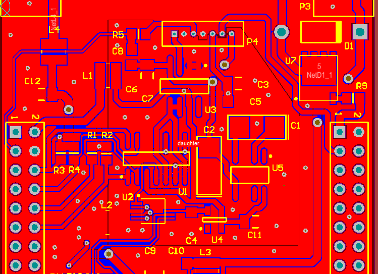
Figure 5: Zoomed view of the top layer.


The 3D render of the board is shown in Figure 6. You can clearly see the pads for the inductor L2 in the lower left. I didn't bother using models for any components unless they were supplied by default, because I have no concern for height tolerances with this board. At this point in the design you may be wondering, why did he only use a single inductor, and not tie the grounds together at multiple points? The short answer is you'd be creating a ground loop, which can be a terrible problem to troubleshoot. You can look up the analysis for ground loops on PCBs, but if you only connect the grounds at one point you won't have to worry about it. You may have other issues, but a ground loop will not be one of them.


image

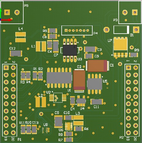
Figure 6: 3D Render of Particle Counter Booster Pack.


Power Supply Decoupling

In my last blog I spoke of decoupling power supplies as well as grounds. I've reproduced the schematic showing these decouplings in Figure 7.

You can see L2 is connecting the grounds, but what about L1; how is that implemented? In the same way. The inductor pads must straddle the gap between the power and signal ground. If you look back at Figure 5, you can clearly see L1 near the upper left straddling the ground boundary.

image

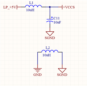
Figure 7: Decoupling inductors


Still Confused?

How about a video explaining it then!


You don't have permission to edit metadata of this video.
Edit media
x
image
Upload Preview
image


Final Remarks

I ordered my board. It was only $10 USD from Seeed Studio for 10 pieces. No one else could compete with that price, so I had to choose them. I've got my bill of materials ready to go, I'm just waiting to hear back about the possibility of samples from TI. Every IC on this board is made by TI, which was a bit of a challenge for me. Hopefully everything can arrive in time to put it together and write some software.

  • Sign in to reply

Top Comments

  • michaelwylie
    michaelwylie over 11 years ago in reply to mcb1 +3
    Mark; Great point. Solder paste is like magic, in the sense that it can fix your mistakes. So, if you happen to slightly misplace a component, the surface tension of the liquifying solder paste will pull…
  • michaelwylie
    michaelwylie over 11 years ago in reply to ipv1 +2
    Yeah, I agree, because most people have already spent most of their budget on getting sensors.
  • michaelwylie
    michaelwylie over 11 years ago in reply to jw0752 +1
    Thanks John and Frederick!
  • amgalbu
    amgalbu over 11 years ago in reply to michaelwylie

    Unfortunately shipping costs outside US are very high... That's a pity because Seeed studio's prices are very competitive

    • Cancel
    • Vote Up 0 Vote Down
    • Sign in to reply
    • More
    • Cancel
  • sleuz
    sleuz over 11 years ago

    Great work and nice content, Michael!


    Thanks for your feedback regarding our PCB service. Our boards are of top quality and come with a high level of service. We also manufacturer and ship directly from Germany, so the price tag is higher than the one from other PCB manufacturers.

    If you need PCBs for other projects in the future, we would be proud to support you.


    Regarding the "graveyard". If you stick to the requirements and standards mentioned in our datasheets, there should be no issues with soldering the parts. The soldering paste and temperatures used are significant and need to be aligned according to the JEDEC soldering standard. If you keep this in mind, you are good.


    Feel free to contact me, if there is anyhting I can do.


    Keep up the good work

    Simon

    • Cancel
    • Vote Up 0 Vote Down
    • Sign in to reply
    • More
    • Cancel
  • shabaz
    shabaz over 11 years ago

    Hi Michael,


    Nice board! Looking forward to seeing it in action!

    • Cancel
    • Vote Up 0 Vote Down
    • Sign in to reply
    • More
    • Cancel
  • michaelwylie
    michaelwylie over 11 years ago in reply to mcb1

    Thanks for asking, I wouldn't have thought to include it otherwise! image

    • Cancel
    • Vote Up +1 Vote Down
    • Sign in to reply
    • More
    • Cancel
  • mcb1
    mcb1 over 11 years ago in reply to michaelwylie

    Michael

    Thanks for the excellent explanation.  Aimage

    I did know what tombstoning was and suspected the idea was to isolate it as per the example ... but wasn't 100%, and now others also know.


    There is obviously some very worthwhile experience, and maybe a challenge involving a design.


    Thanks

    Mark

    • Cancel
    • Vote Up 0 Vote Down
    • Sign in to reply
    • More
    • Cancel
<>
element14 Community

element14 is the first online community specifically for engineers. Connect with your peers and get expert answers to your questions.

  • Members
  • Learn
  • Technologies
  • Challenges & Projects
  • Products
  • Store
  • About Us
  • Feedback & Support
  • FAQs
  • Terms of Use
  • Privacy Policy
  • Legal and Copyright Notices
  • Sitemap
  • Cookies

An Avnet Company © 2026 Premier Farnell Limited. All Rights Reserved.

Premier Farnell Ltd, registered in England and Wales (no 00876412), registered office: Farnell House, Forge Lane, Leeds LS12 2NE.

ICP 备案号 10220084.

Follow element14

  • X
  • Facebook
  • linkedin
  • YouTube