I am very grateful to element14 for giving the opportunity to participate in the Path to Programmable 3 design contest. I will be participating in the ultra96v2 track. I might be a bit late to join the party, but I have a lot of (exciting) things to share in the coming days.
The Kit:
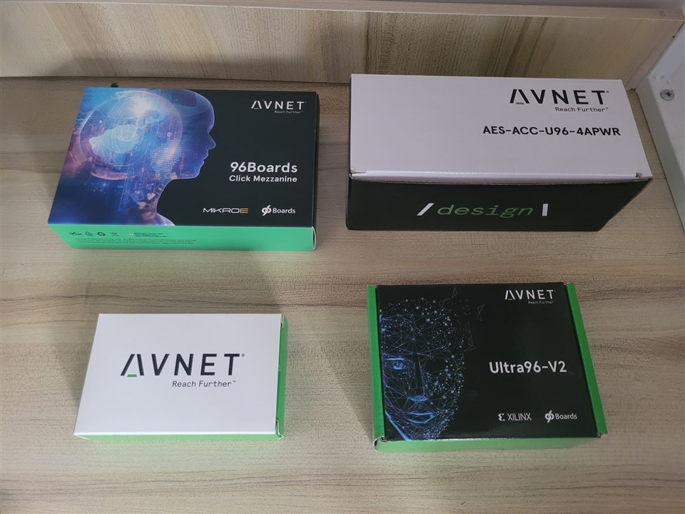
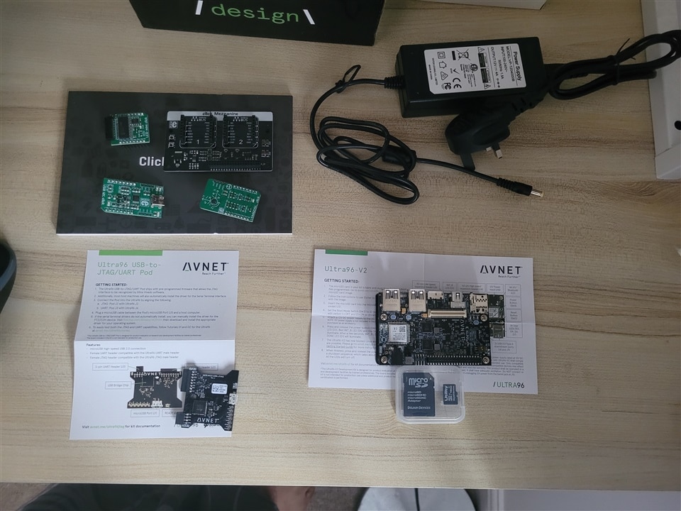
Firstly, I have received the following wonderful set of kits from Element14. I have been looking forward to having a Zynq Ultrascale+ based MPSoC to work on some hobby projects and the project seemed to have started at a great time. All the kits arrived on time and were waiting for me to test them. I received the following.
- Ultra96-v2 MPSoC board with SD card
- Ultra96 USB-to-JTAG/UART Pod
- Power adapter
- Click Mezzanine boards
| Boxes and Unboxing of Ultra96v2 |
|---|
|
Things that I received in the parcel |
|
The interesting bits inside the box |
Connecting bits:
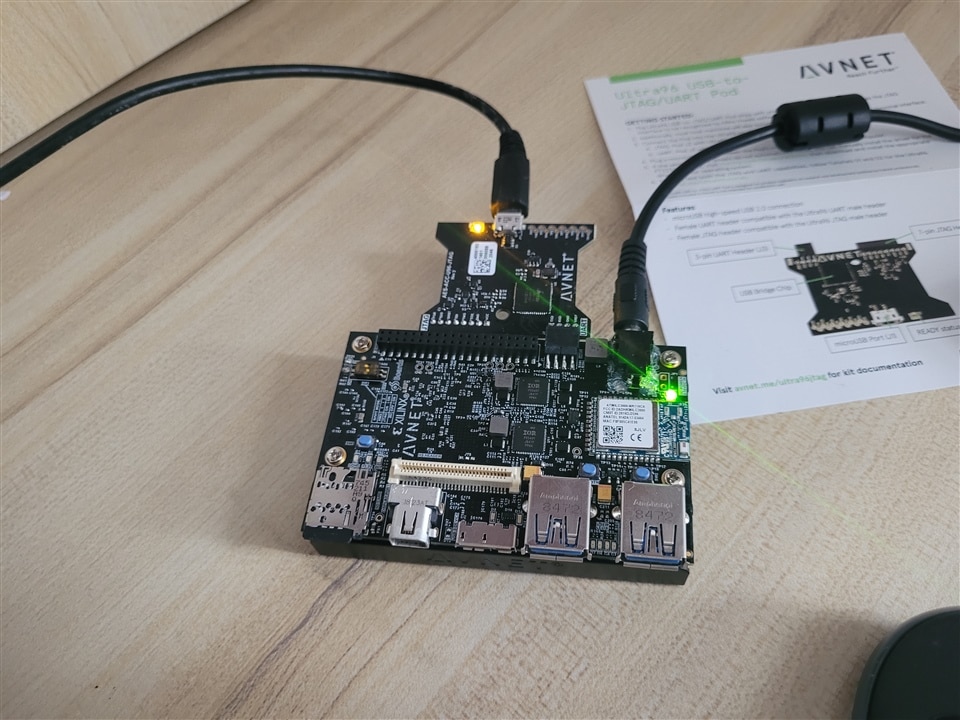
The board came with a very tidy, compact, and well written Getting Started Guide (just to get me started). I just followed the instructions and fetched the boot image and flashed it to the SD card using Balena Etcher tool. Then connected the USB to JTAG/UART pod and powered the unit, noticed the LED beside 12V power input (J10) lit up. Of all the FPGA boards I have used till date, this is the first board that had a Power Button (SW4) to switch it on. I am interested to know if there is any specific reason for it. Obviously, there are both advantages and disadvantages to this approach but will be good to know your thoughts in the comments.

First Boot:
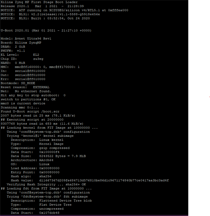
After making sure that boot mode switch is correctly configured, I pressed and released the power button (SW4) and could hear the whirring of the fan, the power on, Init and User LED'S lit as expected. I was also able to see the com port spew out the FSBL, U-BOOT, Kernel and Root FS messages and waited at the login prompt. I was quite happy at this point as that just proves that board is working as expected and I could try my experiments on it in the coming days.

* Video of the boot awaiting approval from moderator.
Tools and Training:
I will be using 2021.2 version of Vivado, Vitis and Petalinux tools installed on a Linux machine (no Virtualbox). The installation was quite seamless and have been playing around with the tools for quite some time and the tools appear to be stable. I have noticed Vivado silently failing because of excess memory usage by during synthesis and timing placement, that too was fixed once the number of jobs allowed to run in parallel was fixed to 4 based on my system requirements. I prefer to script my tool workflows and have a reasonably working configuration that suits my needs which I will be sharing in the upcoming blogs.
I have been following the Ultra96-v2 Training and it has been excellent. I have learned a lot from the lab exercises and participants blogs besides the video tutorials. I will be reinforcing the concepts I have learned in the training in the upcoming blogs.
Future Blogs:
I will be writing four more blogs as part of the training blog series.
Blog 2: Will be focussed on Vivado based HW design. I will be writing about my experience in creating a simplest/minimalistic hardware design with the least amount of peripherals that is sufficient to do a SD card boot. I will be comparing this design against the reference u96v2_sbc_base design by exploring the design and building the design from the Avnet repository,
Blog 3: Will be focussed on Petalinux. I will use the above .xsa file from the above minimalistic hardware design to configure and build a Petalinux system. I will be configuring the rootfs to my requirements, examining the build outputs to validate our modifications.
Blog 4: Will be focussed on Vitis. I will be using the .xsa to run some simple programs, validate the memory using memory tests, debug FSBL and generate application specific .elf that can be run on SD boot.
Blog 5: Create a simple example design that exercises all of the above and hopefully show something in the Display.
Thanks for reading. Will follow up with the other blogs soon.


-

prashanthgn.engineer
-
Cancel
-
Vote Up
0
Vote Down
-
-
Sign in to reply
-
More
-
Cancel
Comment-

prashanthgn.engineer
-
Cancel
-
Vote Up
0
Vote Down
-
-
Sign in to reply
-
More
-
Cancel
Children