


This is my Fourth training blog as part of the Path to Programmable 3 design challenge. As mentioned in the First Blog, this blog will be focussed on Vitis. I will give an overview about Vitis, its features. Then we will be using the .xsa generated in previous blogs to run some simple programs like hello world, peripheral tests, validate the memory using memory tests, and generate application specific .elf that can be run on SD boot.
Vitis Introduction:
Vitis is an advanced development platform created by AMD for FPGAs and adaptive System-on-Chip (SoC) solutions. Vitis is designed to empower software and hardware developers to accelerate and optimize their applications for AMD FPGA and SoC devices.
The Vitis platform offers a unified development environment that streamlines the process of creating high-performance, low-latency, and power-efficient applications targeting AMD devices. It combines software programmability with hardware acceleration, allowing developers to leverage the full potential of FPGA technology without the need for deep hardware design expertise.
In the following sections, we will build some basic applications on Vitis
Platform project:

In the context of AMD Vitis, a Platform Project is a specific type of project used to target a particular AMD hardware platform, such as an FPGA or an SoC device. It provides a pre-configured environment and settings that enable developers to build and deploy applications optimized for that specific hardware target.
Vitis Platform Projects typically include the following components:
-
Hardware Description: This part of the project involves specifying the hardware platform's details, including the target FPGA or SoC device, memory configurations, clock settings, and interconnections. It can include hardware description languages (HDL) like VHDL or Verilog or use higher-level design descriptions like IP Integrator in the Vivado Design Suite.
-
Software Components: Platform Projects include software components, such as device drivers and runtime libraries, that allow software applications to interface with the hardware accelerators created on the FPGA or ACAP. These components are crucial for efficiently offloading computational tasks to the programmable logic.
-
Linker Script and Platform Configurations: The project includes linker scripts that dictate how the software interacts with the hardware accelerators. Additionally, platform-specific configurations are set to optimize the communication between the software and hardware components.
-
Pre-compiled Libraries: Some platform projects may include pre-compiled hardware libraries and functions that developers can use to accelerate specific tasks in their applications.
Vitis Platform Projects are an essential part of the Vitis development flow. They provide a way to encapsulate the hardware and software components specific to a target platform, allowing developers to focus on application development and leverage the full potential of AMD FPGAs and SoCs without dealing with low-level hardware design intricacies.
When a developer creates an application using the Vitis development platform, they start with a Platform Project that matches their target hardware. This ensures that the application is optimized for the specific Xilinx device and can take full advantage of the hardware acceleration capabilities offered by the FPGA or SoC.
Below we build the hardware platform based on the .xsa generated for the minimal Ultra96-v2 design in the previous blogs.

Applicaton projects:
Developers use Vitis Application Projects to create software applications that leverage the power of FPGA or SoC hardware acceleration. By separating the application code from the hardware-specific details, Vitis enables developers to focus on the high-level software design while ensuring efficient hardware-software interaction through the Vitis Platform Project.
When a Vitis Application Project is built, the software code is compiled into an executable that runs on the processor of the target platform. The host code manages the communication with the hardware accelerators (kernels) in the FPGA or SoC, allowing the application to take advantage of the accelerated computation for performance improvements. In the following section we will look at some simple application projects, their purpose, how to build and run them in the hardware.
A simple hello world Vitis application for minimalistic build:
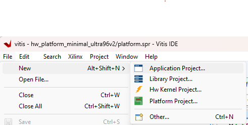
Let us start with a simple hello world application. To create a application select File -> New -> Application Project
Selecting the .xsa file that is corresponding to the minimalistic hw design file that was created in Blog 2.

Providing the name for the project that is clear and precise.

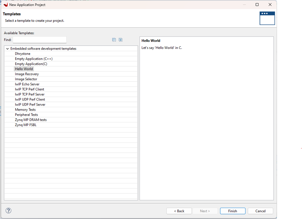
Vitis provides various application templates that we can choose from. In this case we will be choosing the Hello World template. We can start from an empty application as shown in the tutorial too or any other template based on your interest.
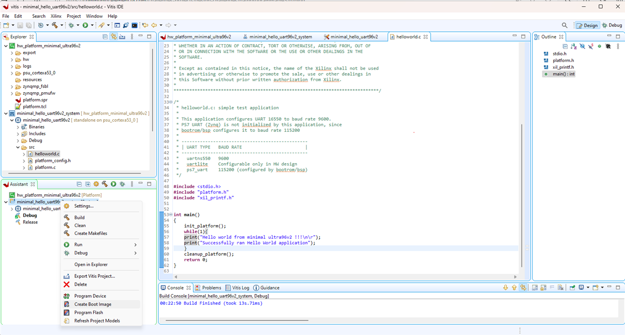
After selecting a template, we also have the ability to modify the template based on our needs. This is very useful for customisation. I have changed the text for the print for this case.

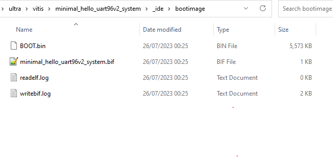
The next step is to build the project and create the BOOT.BIN file so that it can be loaded into the SD card for the SD card boot mode. We can also switch the mode pins to select the JTAG boot mode and program it via JTAG. Since I wanted to test the SD card boot mode, I will stick with the default setting.
Make sure that the Boot image was successfully generated as shown in the console output.

The next step is to copy the BOOT.Bin image to an SD card and try it on the unit.
The last step is to test the BOOT.bin on the board and make sure it prints as expected.

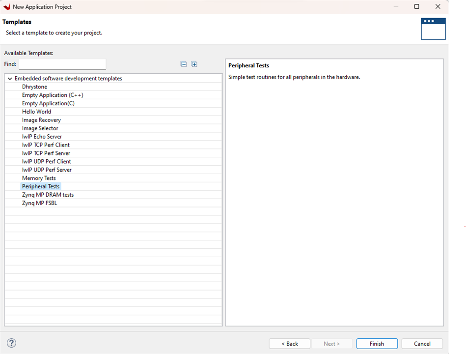
Application to do Peripheral tests
I just following the standard steps for building an application. In this case, I chose the Peripheral tests template.
The tests ran a dozen self tests as expected. It also monitored the temperature of the system using sysmon. So overall happy with the state of affairs for this test.
Xilinx Zynq MP First Stage Boot Loader
Release 2021.2   Jul 26 2023  -  00:10:22
PMU-FW is not running, certain applications may not be supported.
---Entering main---

 Running ScuGicSelfTestExample() for psu_acpu_gic...
ScuGicSelfTestExample PASSED
ScuGic Interrupt Setup PASSED

 Running XZDma_SelfTestExample() for psu_adma_0...
XZDma_SelfTestExample PASSED

 Running Interrupt Test  for psu_adma_0...
ZDMA Simple Example PASSED

 Running XZDma_SelfTestExample() for psu_adma_1...
XZDma_SelfTestExample PASSED

 Running Interrupt Test  for psu_adma_1...
ZDMA Simple Example PASSED

 Running XZDma_SelfTestExample() for psu_adma_2...
XZDma_SelfTestExample PASSED

 Running Interrupt Test  for psu_adma_2...
ZDMA Simple Example PASSED

 Running XZDma_SelfTestExample() for psu_adma_3...
XZDma_SelfTestExample PASSED

 Running Interrupt Test  for psu_adma_3...
ZDMA Simple Example PASSED

 Running XZDma_SelfTestExample() for psu_adma_4...
XZDma_SelfTestExample PASSED

 Running Interrupt Test  for psu_adma_4...
ZDMA Simple Example PASSED

 Running XZDma_SelfTestExample() for psu_adma_5...
XZDma_SelfTestExample PASSED

 Running Interrupt Test  for psu_adma_5...
ZDMA Simple Example PASSED

 Running XZDma_SelfTestExample() for psu_adma_6...
XZDma_SelfTestExample PASSED

 Running Interrupt Test  for psu_adma_6...
ZDMA Simple Example PASSED

 Running XZDma_SelfTestExample() for psu_adma_7...
XZDma_SelfTestExample PASSED

 Running Interrupt Test  for psu_adma_7...
ZDMA Simple Example PASSED

 Running SysMonPsuPolledPrintfExample() for psu_ams...

Entering the SysMon Polled Example.

The Current Temperature is 27.544 Centigrades.
The Maximum Temperature is 28.103 Centigrades.
The Minimum Temperature is 27.124 Centigrades.

The Current Supply 1 is 0.841 Volts.
The Maximum Supply 1 is 0.842 Volts.
The Minimum Supply 1 is 0.840 Volts.

The Current Supply 3 is 1.800 Volts.
The Maximum Supply 3 is 1.802 Volts.
The Minimum Supply 3 is 1.798 Volts.

Exiting the SysMon Polled Example.
SysMonPsuPolledPrintfExample PASSED

 Running SysMonPsuIntrExample()  for psu_ams...

Entering the SysMonPsu Interrupt Example.

The Current Temperature is 27.591 Centigrade.

The Current Supply 1 is 0.840 Volts.

The Current Supply 3 is 1.799 Volts.

Temperature Alarm(0) HIGH Threshold is 17.589 Centigrade.
Temperature Alarm(0) LOW Threshold is 7.587 Centigrade.
Supply 1 Alarm(1) HIGH Threshold is 0.640 Volts.
Supply 1 Alarm(1) LOW Threshold is 1.040 Volts.
Supply 3 Alarm(3) HIGH Threshold is 1.599 Volts.
Supply 3 Alarm(3) LOW Threshold is 1.999 Volts.

Alarm 0 - Temperature alarm has occurred

The Current Temperature is 28.111 Centigrade.
The Maximum Temperature is 28.578 Centigrade.
The Minimum Temperature is 27.544 Centigrade.

The Current Supply 1 is 0.841 Volts.
The Maximum Supply 1 is 0.842 Volts.
The Minimum Supply 1 is 0.840 Volts.

The Current Supply 3 is 1.800 Volts.
The Maximum Supply 3 is 1.802 Volts.
The Minimum Supply 3 is 1.799 Volts.

Exiting the SysMon Interrupt Example.
SysMonPsu IntrExample PASSED

 Running XCsuDma_SelfTestExample() for psu_csudma...
XCsuDma_SelfTestExample PASSED

 Running Interrupt Test  for psu_csudma...
CSUDMA Interrupt Example PASSED

 Running XZDma_SelfTestExample() for psu_gdma_0...
XZDma_SelfTestExample PASSED

 Running Interrupt Test  for psu_gdma_0...
ZDMA Simple Example PASSED

 Running XZDma_SelfTestExample() for psu_gdma_1...
XZDma_SelfTestExample PASSED

 Running Interrupt Test  for psu_gdma_1...
ZDMA Simple Example PASSED

 Running XZDma_SelfTestExample() for psu_gdma_2...
XZDma_SelfTestExample PASSED

 Running Interrupt Test  for psu_gdma_2...
ZDMA Simple Example PASSED

 Running XZDma_SelfTestExample() for psu_gdma_3...
XZDma_SelfTestExample PASSED

 Running Interrupt Test  for psu_gdma_3...
ZDMA Simple Example PASSED

 Running XZDma_SelfTestExample() for psu_gdma_4...
XZDma_SelfTestExample PASSED

 Running Interrupt Test  for psu_gdma_4...
ZDMA Simple Example PASSED

 Running XZDma_SelfTestExample() for psu_gdma_5...
XZDma_SelfTestExample PASSED

 Running Interrupt Test  for psu_gdma_5...
ZDMA Simple Example PASSED

 Running XZDma_SelfTestExample() for psu_gdma_6...
XZDma_SelfTestExample PASSED

 Running Interrupt Test  for psu_gdma_6...
ZDMA Simple Example PASSED

 Running XZDma_SelfTestExample() for psu_gdma_7...
XZDma_SelfTestExample PASSED

 Running Interrupt Test  for psu_gdma_7...
ZDMA Simple Example PASSED

 Running IicPsSelfTestExample() for psu_i2c_1...
IicPsSelfTestExample PASSED
---Exiting main---
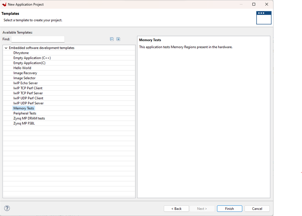
Memory Tests:
I tried to do the memory tests by selecting the Memory Tests template and proceeded with building the application and generating the SD card outputs.
The UART console shows that code didn't proceed beyond the FSBL stage. So the memory tests couldn't be run. I remember during the training section there was a topic specifically intended to show where the application is supposed to run. In the current state, the application is supposed to be running in the OCM, it was not clear if the application needs to be run from the DDR. I expect it should not be running from the DDR as we are intending to test the DDR. I will have to investigate this further. Would be interesting to know if any other participant tried the DDR tests on the Ultra96-v2 board and successfully ran the memory tests.
▒Xilinx Zynq MP First Stage Boot Loader
Release 2021.2   Jul 26 2023  -  00:10:22
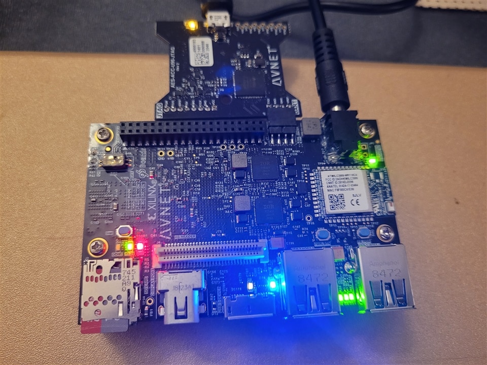
The FPGA board was also not in a happy state as the INIT led were all red :-(
Thanks for reading.