


Exploring Vivado IDE to build the hardware design
Some questions about VIVADO
What is vivado ?
Vivado is a highly complex integrated development environment (IDE) tool for the entire FPGA design and implementation process.
What is HDL (hardware description language) ?
In computer engineering, a hardware description language (HDL) is a specialized computer language used to describe the structure and behavior of electronic circuits, and most commonly, digital logic circuits.
What is Vivado Design Suite ?
Vivado Design Suite is a software suite produced by Xilinx for synthesis and analysis of hardware description language (HDL) designs, with additional features for system on a chip development and high-level synthesis.
What is a Vivado High-Level Synthesis compiler ?
The Vivado High-Level Synthesis compiler enables C, C++ and SystemC programs to be directly targeted into Xilinx devices without the need to manually create RTL.[
What is vivado HLS ?
Vivado HLS is widely reviewed to increase developer productivity, and is confirmed to support C++ classes, templates, functions and operator overloading.
What is OpenCL kernal ?
OpenCL kernels are programs that execute across various CPU, GPU and FPGA platforms.[16][19]
What is Vivado simulator ?
The Vivado Simulator is a component of the Vivado Design Suite. It is a compiled-language simulator that supports mixed-language, Tcl scripts, encrypted IP and enhanced verification.
What is Vivado IP integrator ?
The Vivado IP Integrator allows engineers to quickly integrate and configure IP from the large Xilinx IP library. The Integrator is also tuned for MathWorks Simulink designs built with Xilinx's System Generator and Vivado High-Level Synthesis.
What is Vivado system generator ?
Vivado system generator is a design tool in the Vivado® Design Suite that enables you to use the MathWorks® model-based Simulink® design environment for FPGA design.
What is vivado TCL store ?
The Vivado Tcl Store is a scripting system for developing add-ons to Vivado, and can be used to add and modify Vivado's capabilities.[19] Tcl is the scripting language on which Vivado itself is based.[19] All of Vivado's underlying functions can be invoked and controlled via Tcl scripts.
Learning about Vivado design flow
What is a design flow ?
Design flows are the explicit combination of electronic design automation tools to accomplish the design of an integrated circuit.
What is a design process ?
The design process is a tool that helps you break down large projects into smaller, easier-to handle stages.
What are the various design process in Xilinx ?
- System and Solution Planning
- Hardware, IP, and Platform Development
- System Integration and Validation
- Board System Design
What is the purpose of System and Solution Planning in design process ?
Identifying the components, performance, I/O, and data transfer requirements at a system level. Includes application mapping for the solution to PS, PL, and AI Engine.
What is the purpose of Hardware, IP, and Platform Development in design process ?
Creating the PL IP blocks for the hardware platform, creating PL kernels, functional simulation, and evaluating the Vivado® timing, resource use, and power closure. Also involves developing the hardware platform for system integration.
What is the purpose of System Integration and Validation in design process ?
Integrating and validating the system functional performance, including timing, resource use, and power closure.
What is the purpose of Board System Design in design process ?
Designing a PCB through schematics and board layout. Also involves power, thermal, and signal integrity considerations.
What are the various design flows in System and Solution Planning design process ?
- Design Flows
- RTL-to-Bitstream Design Flow
- Alternate RTL-to-Bitstream Design Flow
What are the various design flows in Hardware, IP, and Platform Development design process ?
- Accelerated Kernal
What are the various design flows in System Integration and Validation design process ?
- Running Logic simulation
- Logic simulation
What are the various design flows in Board System Design design process ?
- Xilinx Platform Board Support
- Board Files
What is an industry design standard ?
Industry standards are voluntary agreements that establish requirements for products, practices, or operations in a given field.
What are the various industry standard supported by Vivado Design Suite ?
- Tcl
- AXI4,IP-XACT
- Synopsys design constraints (SDC)
- Verilog, VHDL, VHDL-2008, SystemVerilog
- SystemC, C, C++
What is RTL-to-Bitstream Design Flow ?
RTL (register-transfer level) design is a hardware design methodology that describes the behavior of digital circuits in terms of the flow of data between registers, and the operations that are performed on that data as it moves through the circuit.
What are the benefits of using RTL design?
RTL design allows designers to create digital circuits that are easier to understand, debug, and verify. It also allows for faster design iteration, as changes can be made at the RTL level rather than requiring changes to be made at the gate-level.
What tools are used in RTL design?
RTL design typically involves the use of hardware description languages (HDLs) such as VHDL or Verilog, as well as design tools such as synthesis tools and simulation tools.
How does RTL design differ from gate-level design?
RTL design focuses on the behavior of the circuit, whereas gate-level design focuses on the physical implementation of the circuit using logic gates. RTL design is a higher level of abstraction, allowing for easier design and modification, while gate-level design is more detailed and specific.
Can RTL design be used for all types of digital circuits?
RTL design is generally used for digital circuits that are relatively simple and have a small number of inputs and outputs. For more complex circuits, other design methodologies may be more appropriate.
What tools are available in RTL-to-bitstream design flow ?
- RTL Design
- IP Design and System-Level Design Integration
- IP Subsystem Design
- I/O and Clock Planning
- Xilinx Platform Board Support
- Synthesis
- Design Analysis and Simulation
- Placement and Routing
- Hardware Debug and Validation
What is the purpose of ‘RTL Design’ design tool ?
You can specify RTL source files to create a project and use these sources for RTL code development, analysis, synthesis and implementation.
What is the purpose of ‘IP Design and System-Level Design Integration’ design tool ?
The Vivado Design Suite provides an environment to configure, implement, verify, and integrate IP as a standalone module or within the context of the system-level design.
What is the purpose of ‘IP Subsystem Design’ design tool ?
The Vivado IP integrator environment enables you to stitch together various IP into IP subsystems using the AMBA® AXI4 interconnect protocol.
What is the purpose of ‘I/O and Clock Planning’ design tool ?
The Vivado IDE provides an I/O pin planning environment that enables I/O port assignment either onto specific device package pins or onto internal die pads, and provides tables to let you design and analyze package and I/O-related data.
What is the purpose of ‘Xilinx Platform Board Support’ design tool ?
In the Vivado Design Suite, you can select an existing Xilinx evaluation platform board as a target for your design. In the platform board flow, all of the IP interfaces implemented on the target board are exposed to enable quick selection and configuration of the IP used in your design. The resulting IP configuration parameters and physical board constraints, such as I/O standard and package pin constraints, are automatically assigned and proliferated throughout the flow.
What is the purpose of ‘Synthesis’ design tool ?
Vivado synthesis performs a global, or top-down synthesis of the overall RTL design.
What is the purpose of ‘Design Analysis and Simulation’ design tool ?
The Vivado Design Suite lets you analyze, verify, and modify the design at each stage of the design process. You can run design rule and design methodology checks, logic simulation, timing and power analysis to improve circuit performance.
What is the purpose of ‘Placement and Routing’ design tool ?
When the synthesized netlist is available, Vivado implementation provides all the features necessary to optimize, place and route the netlist onto the available device resources of the target part. Vivado implementation works to satisfy the logical, physical, and timing constraints of the design.
What is the purpose of ‘Hardware Debug and Validation’ design tool ?
After implementation, the device can be programmed and then analyzed with the Vivado logic analyzer, or within the standalone Vivado Lab Edition environment. Debug signals can be identified in the RTL design, or inserted after synthesis and are processed throughout the flow. You can add debug cores to the RTL source files, to the synthesized netlist, or in an implemented design using the using the Engineering Change Order (ECO) flow. You can also modify the nets connected to a debug probe, or route internal signals to a package pin for external probing using the ECO flow.
What tools are available in Alternate RTL-to-Bitstream Design Flows ?
- Accelerated Kernel Flows
- Embedded Processor Design
- Model-Based Design Using Model Composer
- Model-Based DSP Design Using Xilinx System Generator
- High-Level Synthesis C-Based Design
- Dynamic Function Exchange Design
- Hierarchical Design
What is the purpose of ‘Accelerated Kernel Flows’ design tool ?
In this design methodology, Vivado is used to create a platform which is consumed by the Vitis software platform to add accelerated kernels. The hardware design is comprised of the platform and the accelerators. In this case, the final bitstream is created by the Vitis software platform because the complete design is not visible in Vivado.
What is the purpose of ‘Embedded Processor Design’ design tool ?
A slightly different tool flow is needed when creating an embedded processor design. Because the embedded processor requires software in order to boot-up and run effectively, the software design flow must work in unison with the hardware design flow. Data hand-off between the hardware and software flows, and validation across these two domains is critical for success.
What is the purpose of ‘Model-Based Design Using Model Composer’ design tool ?
Model Composer is a model-based graphical design tool that enables rapid design exploration within the MathWorks MATLAB® and Simulink® products and accelerates the path to production for Xilinx devices through automatic code generation.
What is the purpose of ‘Model-Based DSP Design Using Xilinx System Generator’ design tool ?
The Xilinx System Generator tool, which is installed as part of the Vivado Design Suite, can be used for implementing DSP functions. You create the DSP functions using System Generator as a standalone tool, and then package your System Generator design into an IP module that can be included in the Vivado IP catalog. From there, the generated IP can be instantiated into your Vivado design as a submodule.
What is the purpose of ‘High-Level Synthesis C-Based Design’ design tool ?
The C-based High-Level Synthesis (HLS) tools within the Vivado Design Suite enable you to describe various DSP functions in the design using C, C++, and SystemC. You create and validate the C code with the Vivado HLS tools. Use of higher-level languages allows you to abstract algorithmic descriptions, data type, specification, etc. You can create “what-if” scenarios using various parameters to optimize design performance and device area. HLS lets you simulate the generated RTL directly from its design environment using C-based test benches and simulation. C-to-RTL synthesis transforms the C-based design into an RTL module that can be packaged and implemented as part of a larger RTL design, or instantiated into an IP integrator block design.
What is the purpose of ‘Dynamic Function Exchange Design’ design tool ?
Dynamic function exchange (DFx) allows portions of a running Xilinx device to be reconfigured in real-time with a partial bitstream, changing the features and functions of the running design. The reconfigurable modules must be properly planned to ensure they function as needed for maximum performance.
The DFx flow requires a strict design process to ensure that the reconfigurable modules are designed properly to enable glitch-less operation during partial bitstream updates. This includes reducing the number of interface signals into the reconfigurable module, floorplanning device resources, and pin placement; as well as adhering to special DFx DRCs. The device programming method must also be properly planned to ensure the configuration I/O pins are assigned appropriately.
What is the purpose of ‘Hierarchical Design’ design tool ?
Hierarchical Design (HD) flows enable you to partition a design into smaller, more manageable modules to be processed independently. The hierarchical design flow involves proper module interface design, constraint definition, floorplanning, and some special commands and design techniques.
Learning about Vivado design suit Models
What is a usage model ?
A usage model is a collection of data that describes system usage within a stated context. The usage model data describe the interactions between the user and the system at a level that identifies the system's benefits to the user.
What is Vivado design Suite Use Models ?
It is a set of design flow and tools that Vivado provides the user for testing their designs.
What is Vivado IDE ?
The Vivado IDE provides an interface to assemble, implement, and validate your design and IP. Opening a design loads the current design netlist, applies design constraints, and fits the design onto the target device.
What are the two modes Vivado IDE can be used in ?
The vivado IDE can be used in Project Mode and Non Project Mode
What is a project mode in vivado IDE ?
In Project Mode, Vivado tools automatically manage your design flow and design data.
What is non project mode in vivado IDE ?
Non-Project Mode enables you to have full control over each design flow step, but you must manually manage source files, reports, and intermediate results known as design checkpoints.
What are the features available in project mode ?
- Out-of-the-box design flow
- Easy-to-use, push-button interface
- Powerful Tcl scripting language for customization
- Source file management and status
- Automatically generated standard reports
- Storage and reuse of tool settings and design configuration
- Experimentation with multiple synthesis and implementation runs
- Run results management and status
What are the features available in non project mode ?
all operations and tool settings require individual Tcl commands, including setting tool options, running implementation commands, generating reports, and writing design checkpoints.
Running Vivado in project mode
In Project Mode, the Vivado® Design Suite creates a project directory structure and automatically manages your source files, constraints, IP data, synthesis and implementation run results, and reports. In this mode, the Vivado Design Suite also manages and reports on the status of the source files, configuration, and the state of the design.
In order to open the Vivado IDE in project mode. Click on Vivado application as shown in figure 1.0 bellow
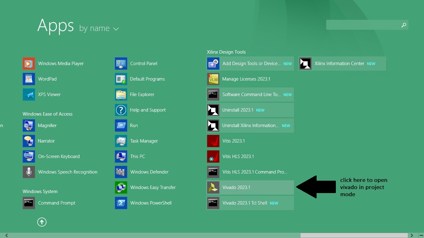
Figure 1.0
After clicking on it an application program will start as shown in figure 1.1 bellow
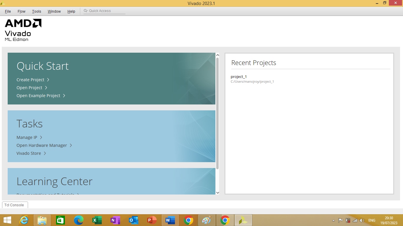
Figure 1.1
Click on create project on quick start block as shown in figure 1.2 bellow
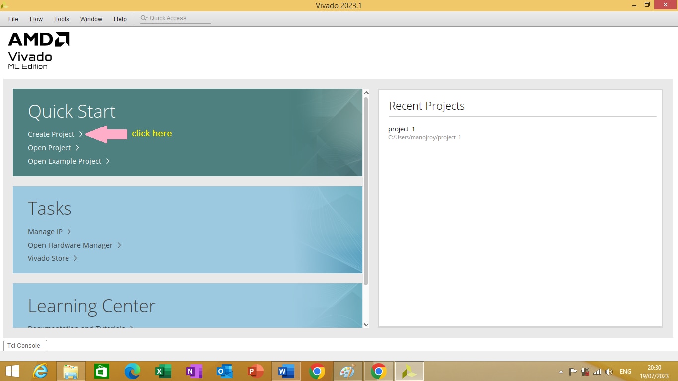
Figure 1.2
After clicking on create project a New project window will open as shown in figure 1.3 bellow
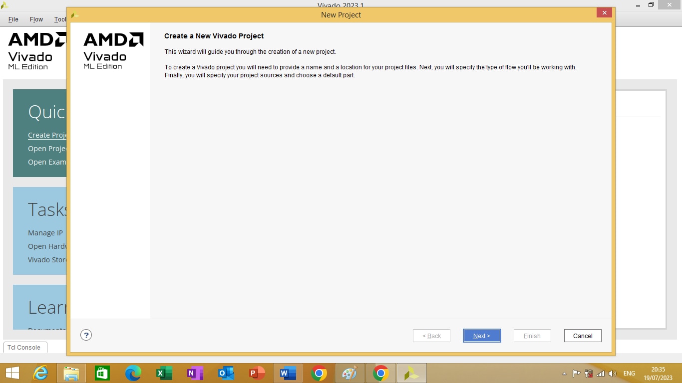
Figure 1.3
Click on next button of new project window a project name window will open as shown in figure 1.4 bellow
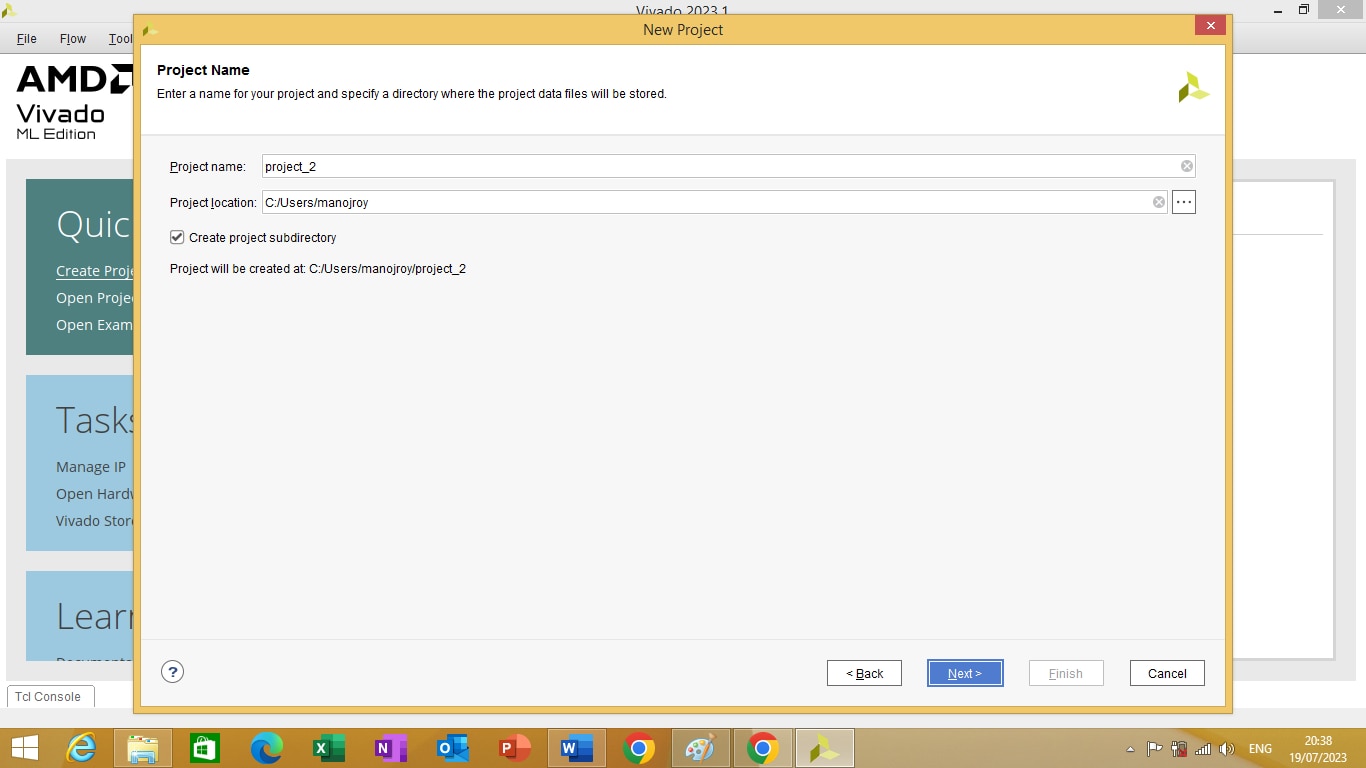
Figure 1.4
On the project name window mention the project name as per your requirement and then click next. A project type window will appear as shown in figure 1.5 bellow
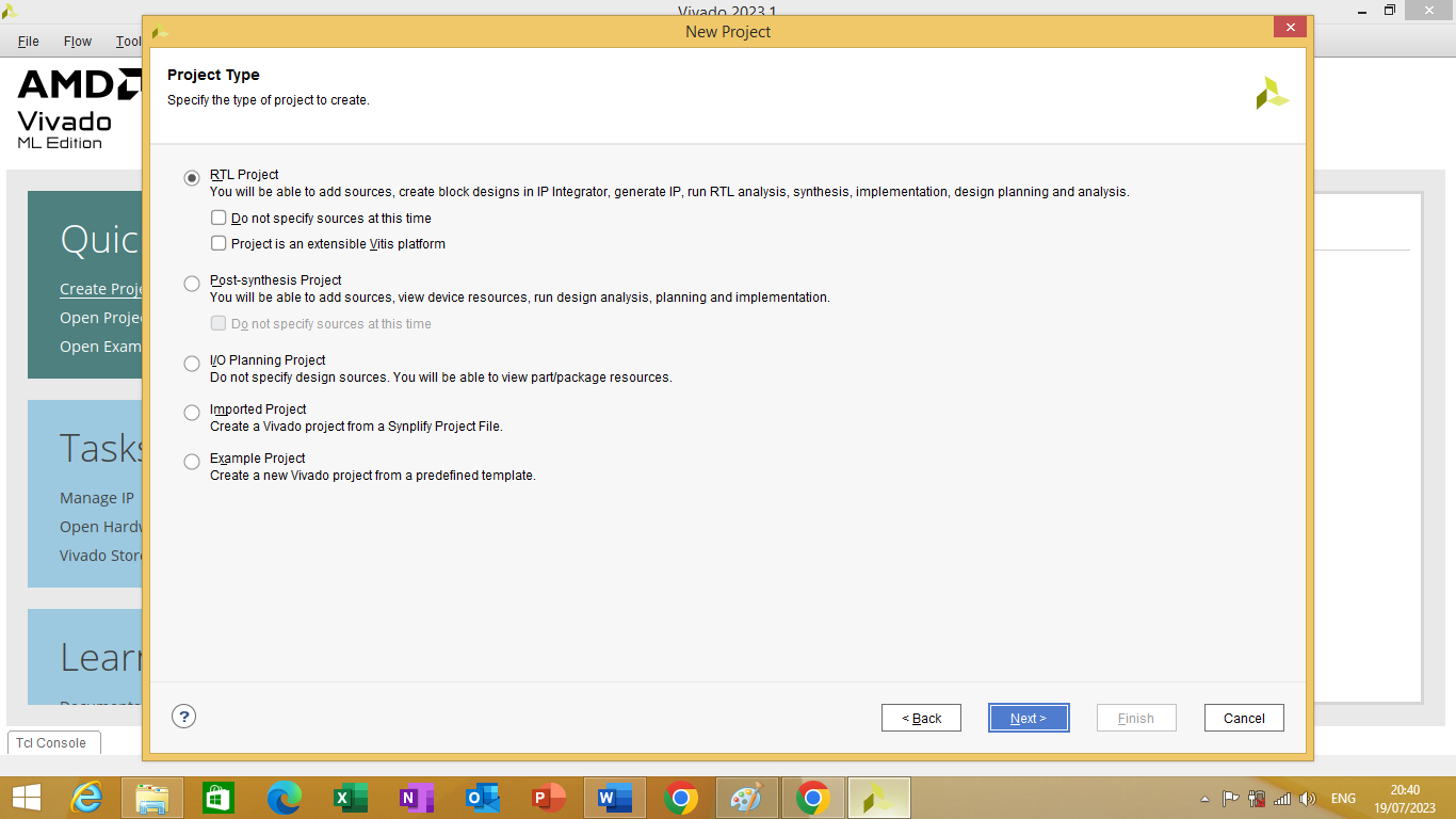
Figure 1.5
On project type window select RTL project and than click next add source window will appear as shown in figure 1.6 bellow
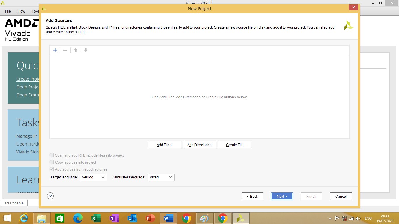
Figure 1.6
Click next button on Add Sources window an Add Constraints window will open as shown in figure 1.7 bellow
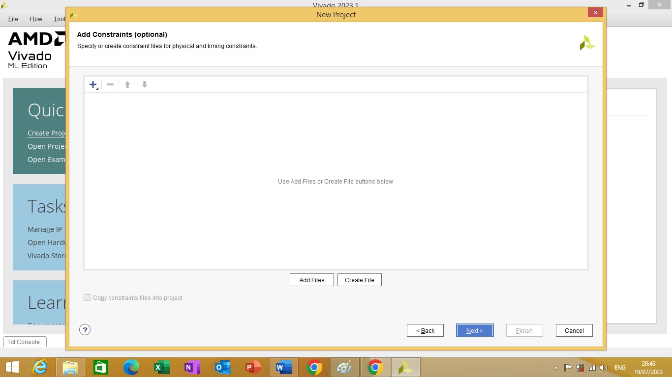
Figure 1.7
Click on next button on Add Constraints window default parts window will appear as shown in figure 1.8 bellow
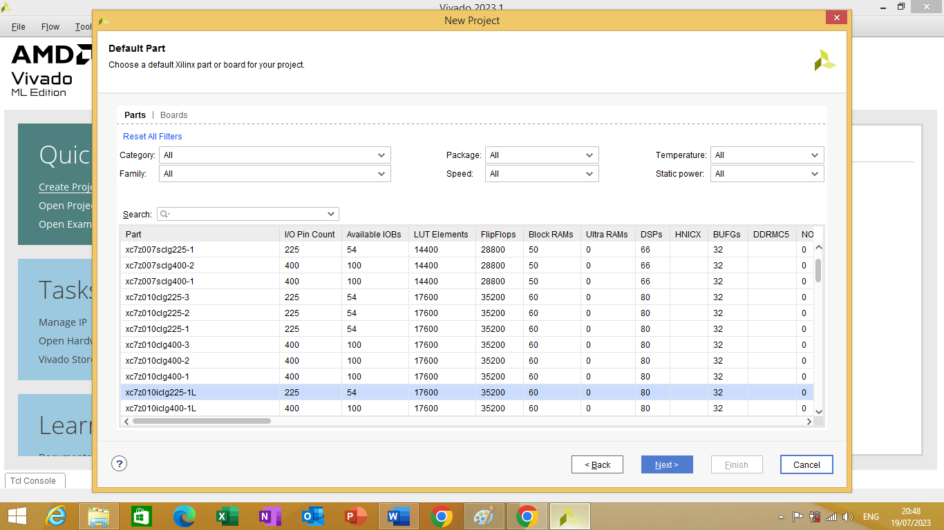
Figure 1.8
Click on boards of Default part window a board window will open as shown in figure 1.9 bellow
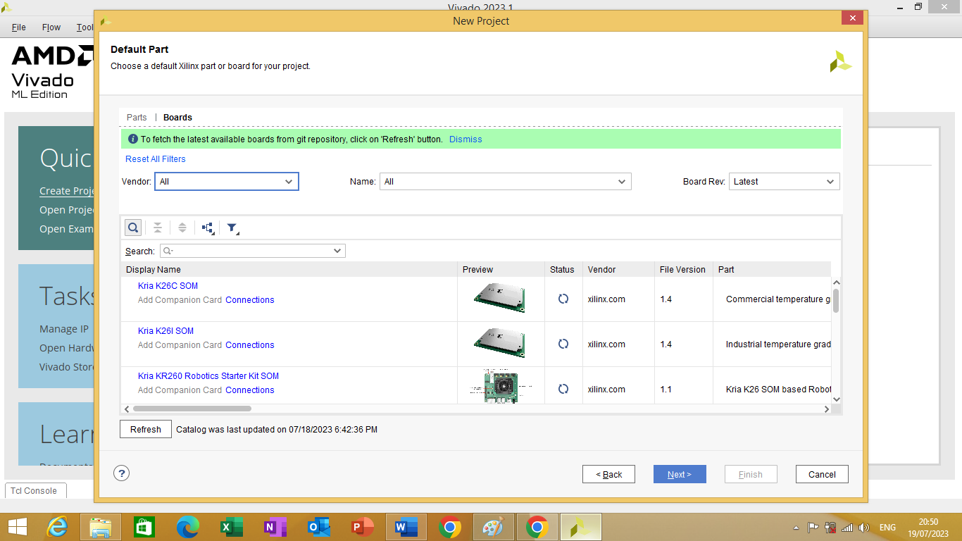
Figure 1.9
Click on refresh to fetch the latest board from git repository. On vendor drop down box select avnet.com. On the name drop down box select Ultra 96 v2 single board computer as shown in figure 1.10 bellow
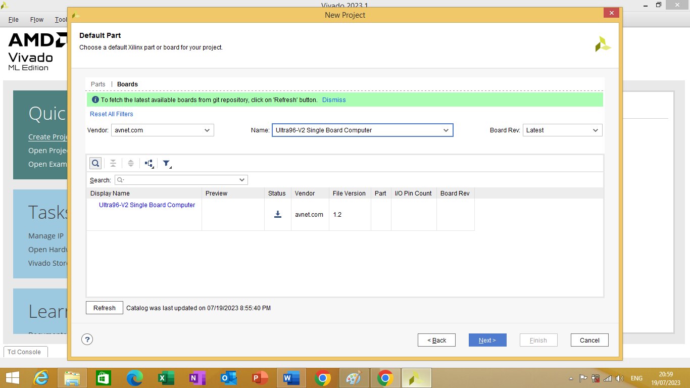
Figure 1.10
Click on download button in the status box to download the Ultra96-v2. After the download happened all the information about the board will be displayed as shown in figure1.11 bellow
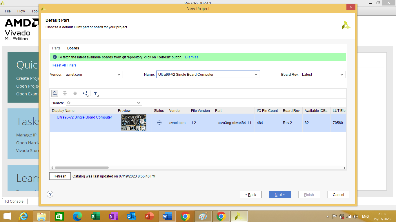
Figure 1.11
Click on next button a ‘New Project Summary’ window will open as shown in figure 1.12 bellow
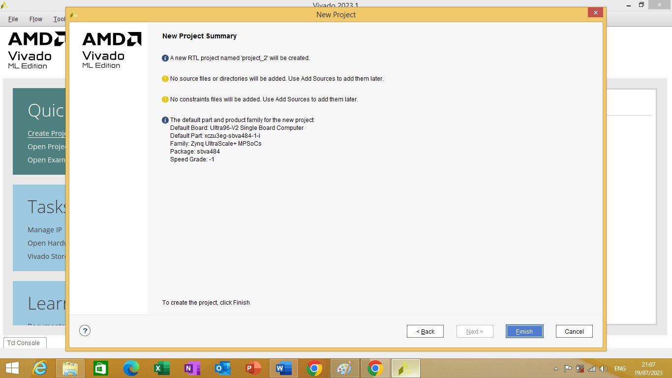
Figure 1.12
Click on finish button project will be created and Vivaldo IDE will open as shown in figure 1.13 bellow
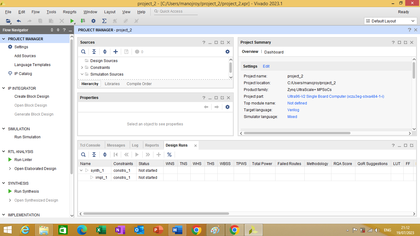
Figure 1.13
Some question with respect to Block design container
What is a Block Design Container in Vivado ML?
Block Design Container (BDC) is a new feature in Vivado IP Integrator which allows one or more block designs to be instantiated inside another block design. This enables a seamless team-based design environment for engineers who work on parts of a bigger design. BDC also provides a project-based approach to enable and disable DFX (formerly called Partial
What is a Block Design ?
Block Designs are complex subsystem designs made up of interconnected IP cores, that can either serve as stand-alone designs, or be integrated into other designs. Block Designs, or diagrams, can be created with the IP integrator of the Vivado Design Suite. They can be created interactively, on the canvas of the IP integrator in the Vivado Design Suite IDE, or interactively using Tcl commands.
What is the purpose of Block Design ?
A block design provides a visual representation of your hardware design, and can be used to easily connect and configure IP cores.
Experimenting with block design
To start creating block design click on ‘Create block Design’ in ‘IPINTEGRATOR’ drop down arrow as shown in figure 2.0 bellow

Figure 2.0
After clicking on ‘Create block design’ a Create Block Design window will open as shown in figure 2.1 bellow
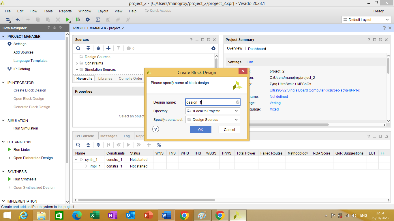
Figure 2.1
Mention the design name in design text box and than click ‘ok’ a block design window will open as shown in figure 2.2 bellow
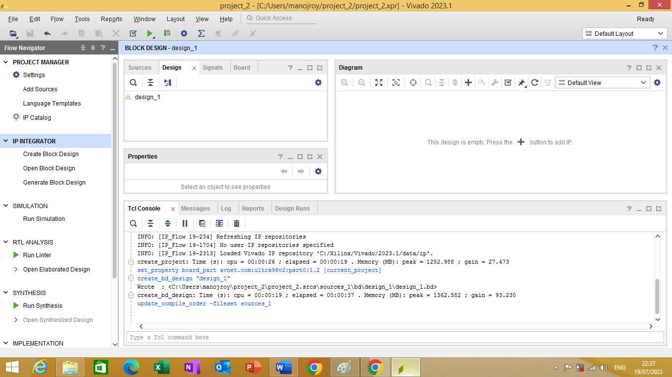
Figure 2.2
After opening the block design window you need to add IP blocks in it. To add IP block click on + button on diagram window as shown in figure 2.3 bellow
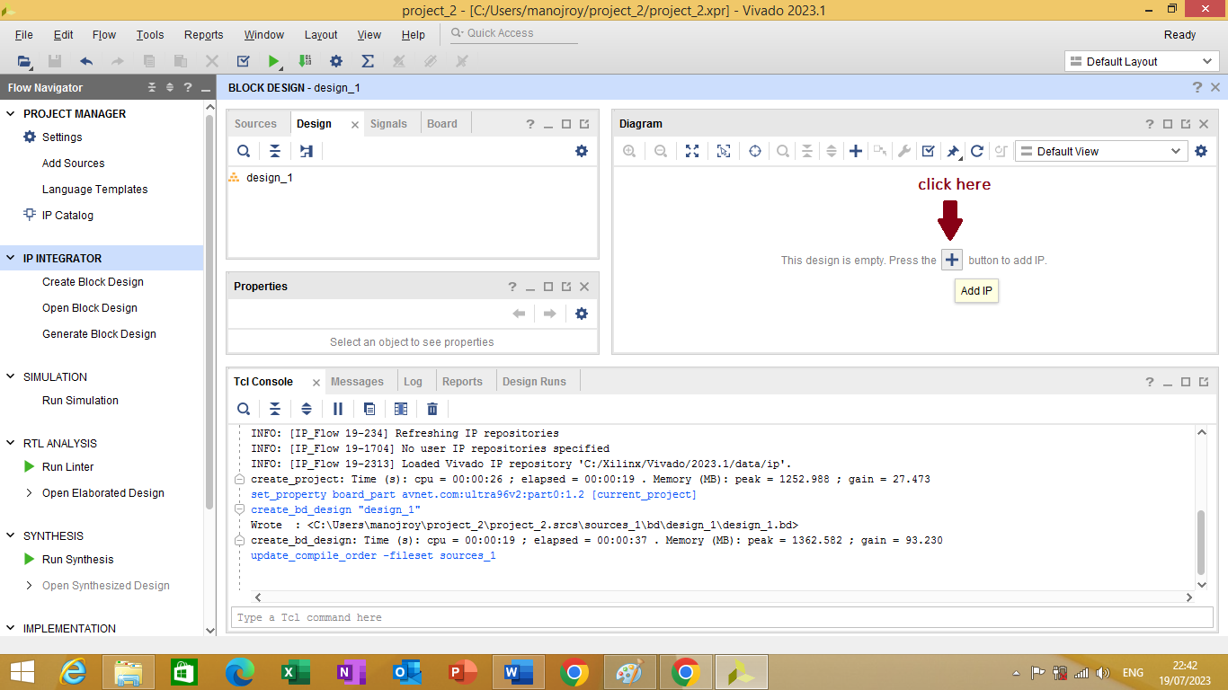
Figure 2.3
After clicking on it an IP window will open which has a list of IP as shown in figure 2.4 bellow
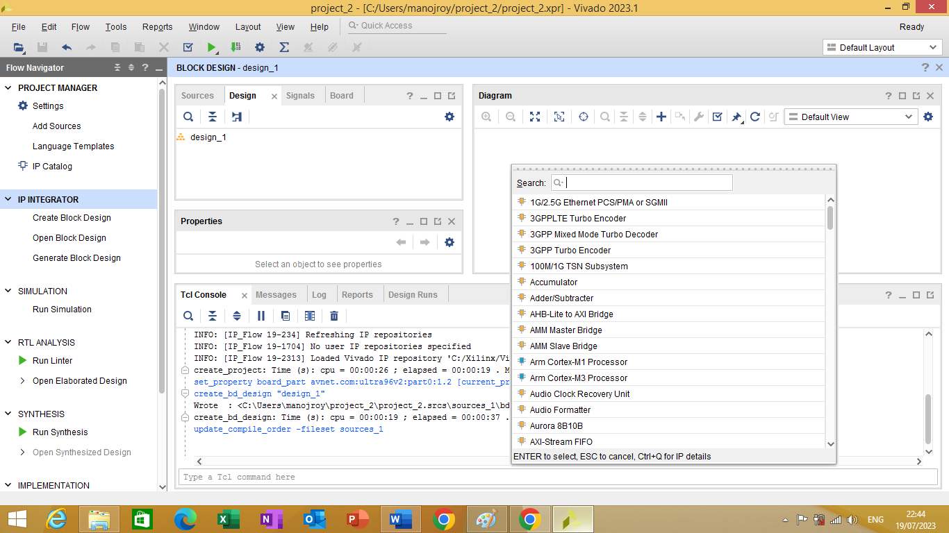
Figure 2.4
In the IP window search for ZYNQ Ultrascale+ MPSoC as shown in figure 2.5 bellow
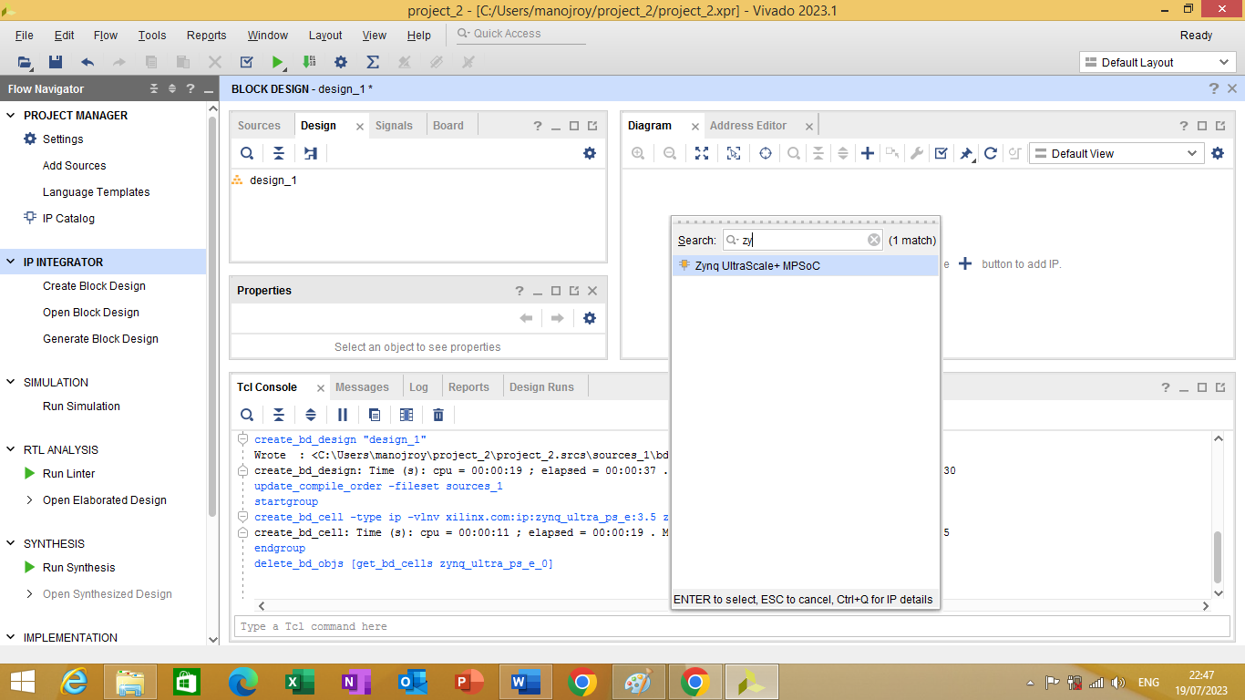
Figure 2.5
Double Click on ZYNQ Ultrascale+ MPSoC to load the IP as shown in figure 2.6 bellow
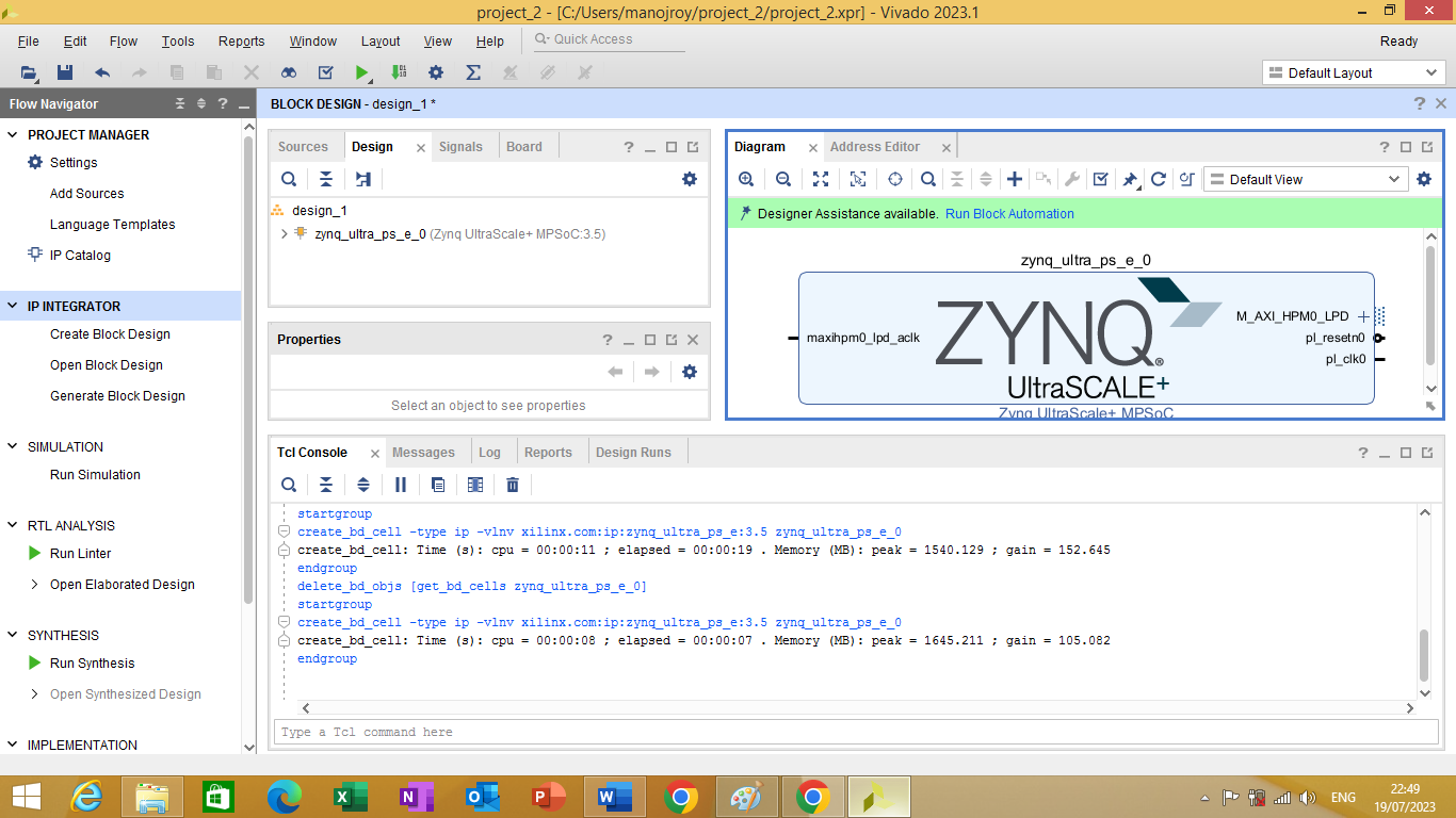
Figure 2.6
The block is unconfigured right know. To configure the block click on Run Block Automation as shown in figure 2.7 bellow
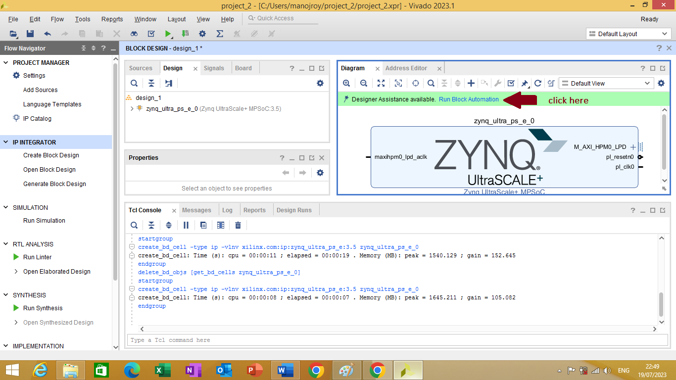
Figure 2.7
After clicking on it Run Block Automation window will open as shown in figure 2.8 bellow
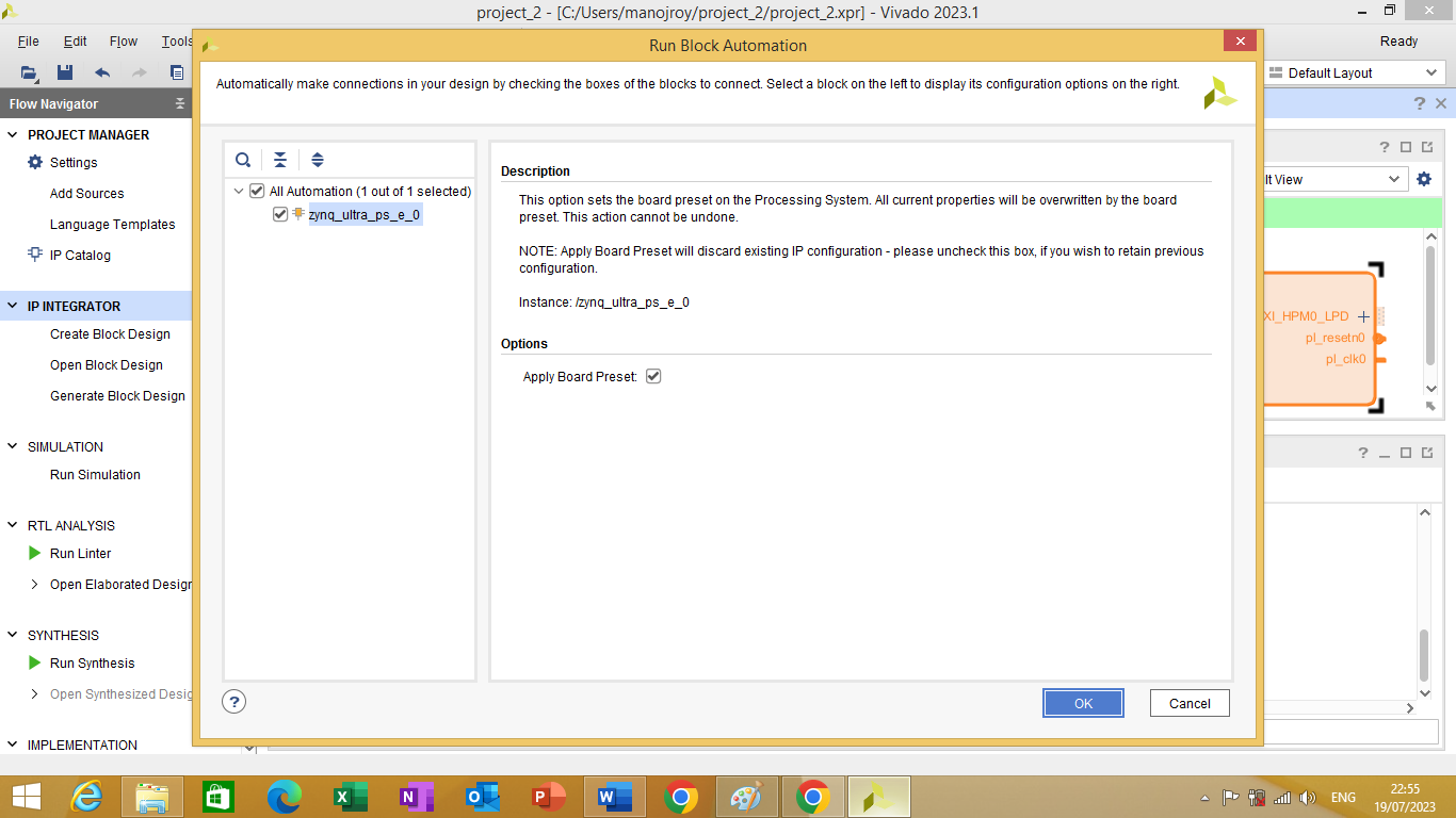
Figure 2.8
On this window check All automation box and than click OK button
The two clock ports on the left side maxihpm0_fpd_aclk and maxihpm1_fpd_aclk must have a clock connected to them. To do this, we can connect them to pl_clk0 clock output from the Zynq block. To make the connection, click and drag the mouse from the pl_clk0 port's pin to the other two ports' pins.
As shown in figure 2.9 bellow
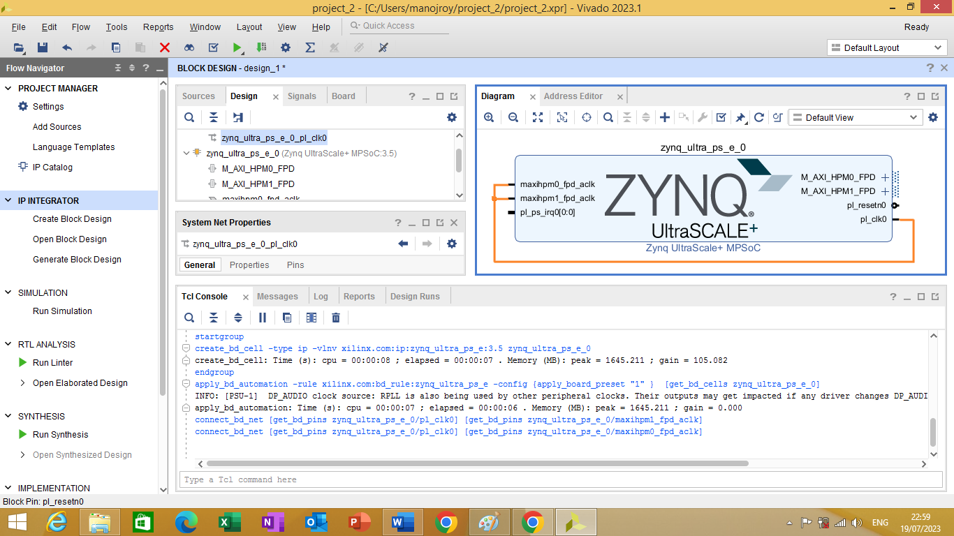
Figure 2.9
After connection you need to validate the design. To validate the design click on validation button on diagram window as shown in figure 2.10 bellow
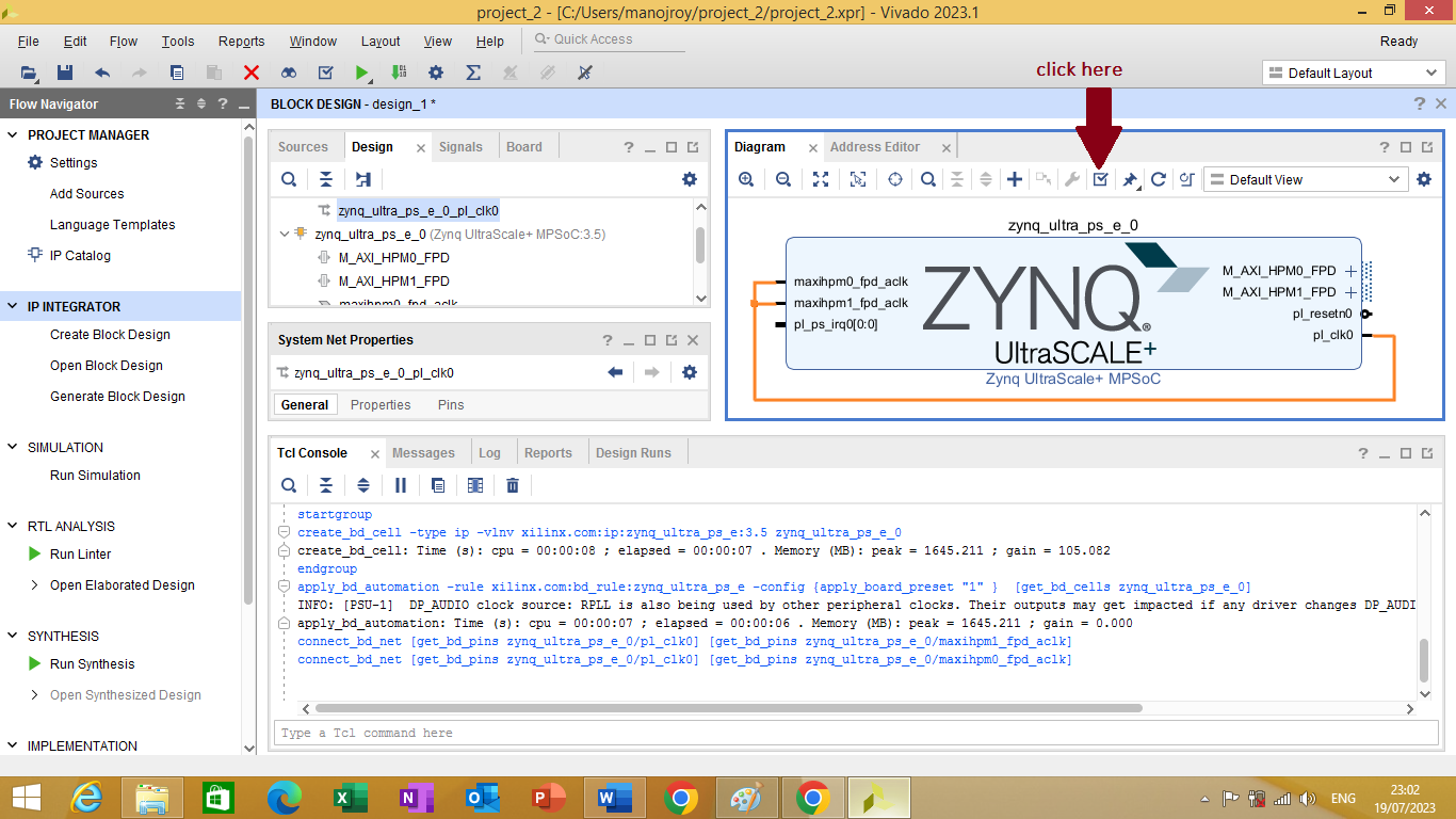
Figure 2.10
Now we need to create an HDL Wrapper(Note:- HDL Wrapper translates the block design into a source file that can be read by the Vivado tools, and is used to build the actual design.) To create HDL Wrapper click on Source Tab of Block window as shown in figure 2.11 bellow
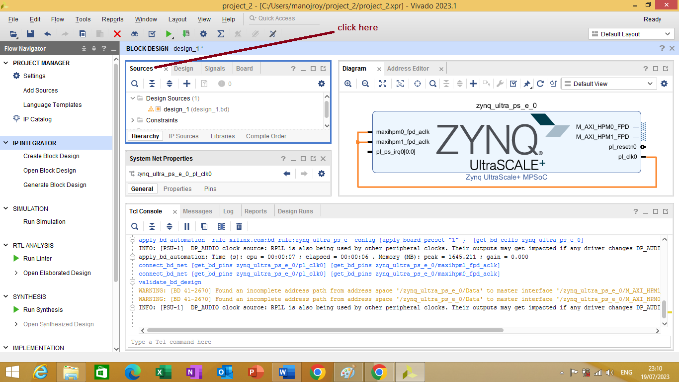
Figure 2.11
And then right click on ‘design_1’ element and then select ‘Create HDL Wrapper’ as shown in figure 2.12 bellow
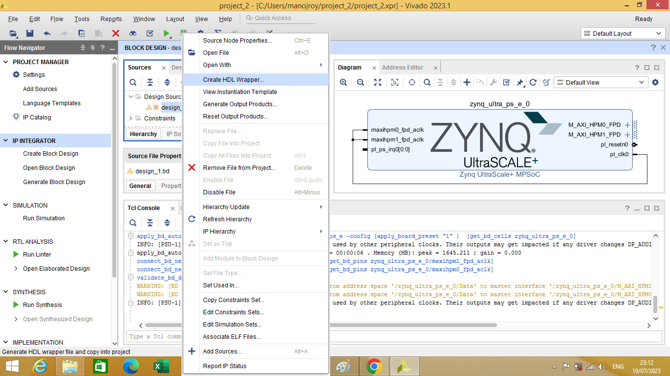
Figure 2.12
After clicking on it Create HDL Wrapper window will open as shown in figure 2.13 bellow
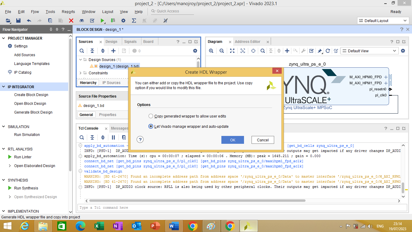
Figure 2.13
Click on Let Vivado manage wrapper and auto-update bullet and then click OK. Know you need to generate bitstream and export platform for Vitis IDE. To generate bitstream go to Program and debug in flow navigation window and than click on generate bitstream as shown in figure 2.14 bellow
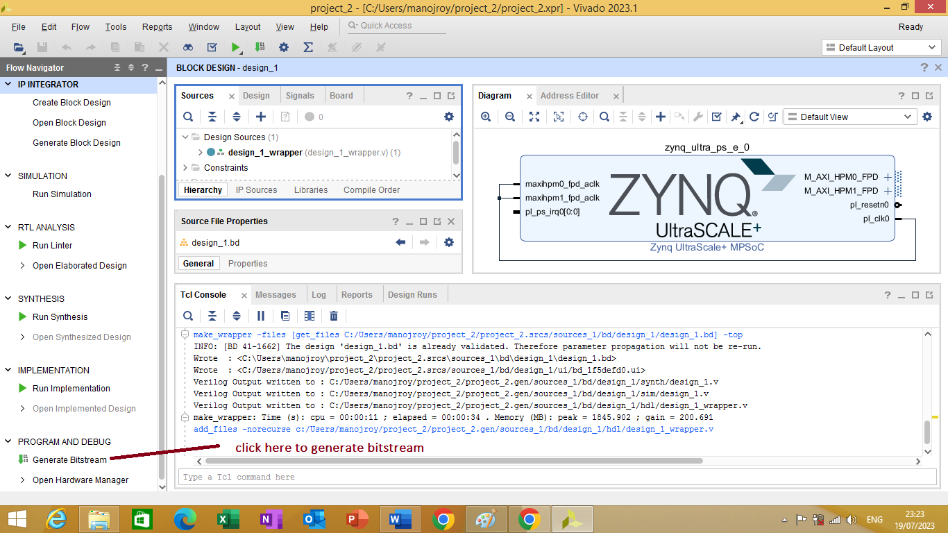
Figure 2.14
Clicking on it will generate bitstream. Now we will export our hardware platform to Vitis
To do Click File -> Export -> Export Hardware. as shown in figure 2.15 bellow

Figure 2.15
This will open the Export hardware platform as shown in figure 2.16 bellow
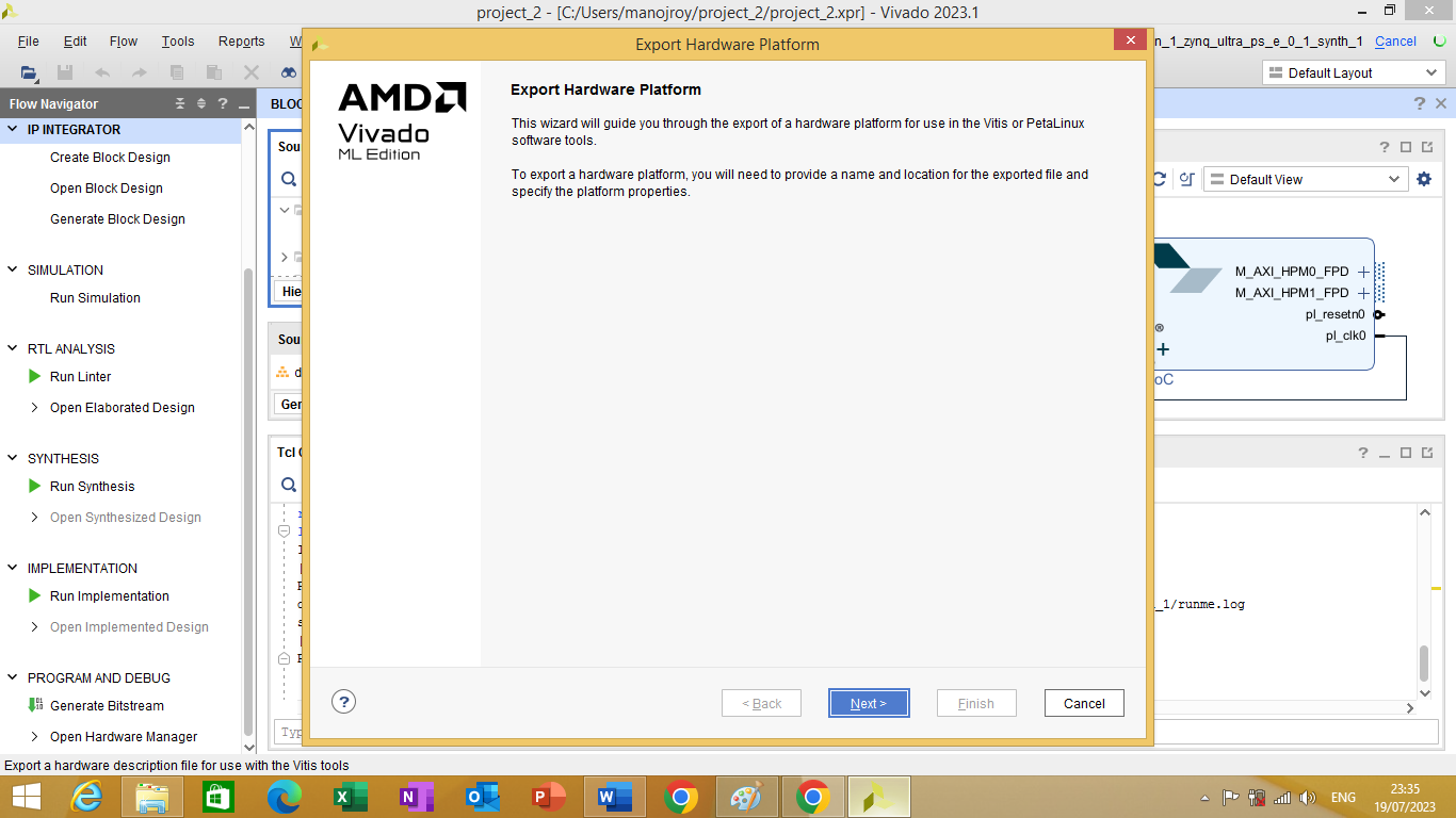
Figure 2.16
Click next output window will open. Click on Include bitstream bullet as shown in figure 2.17 bellow
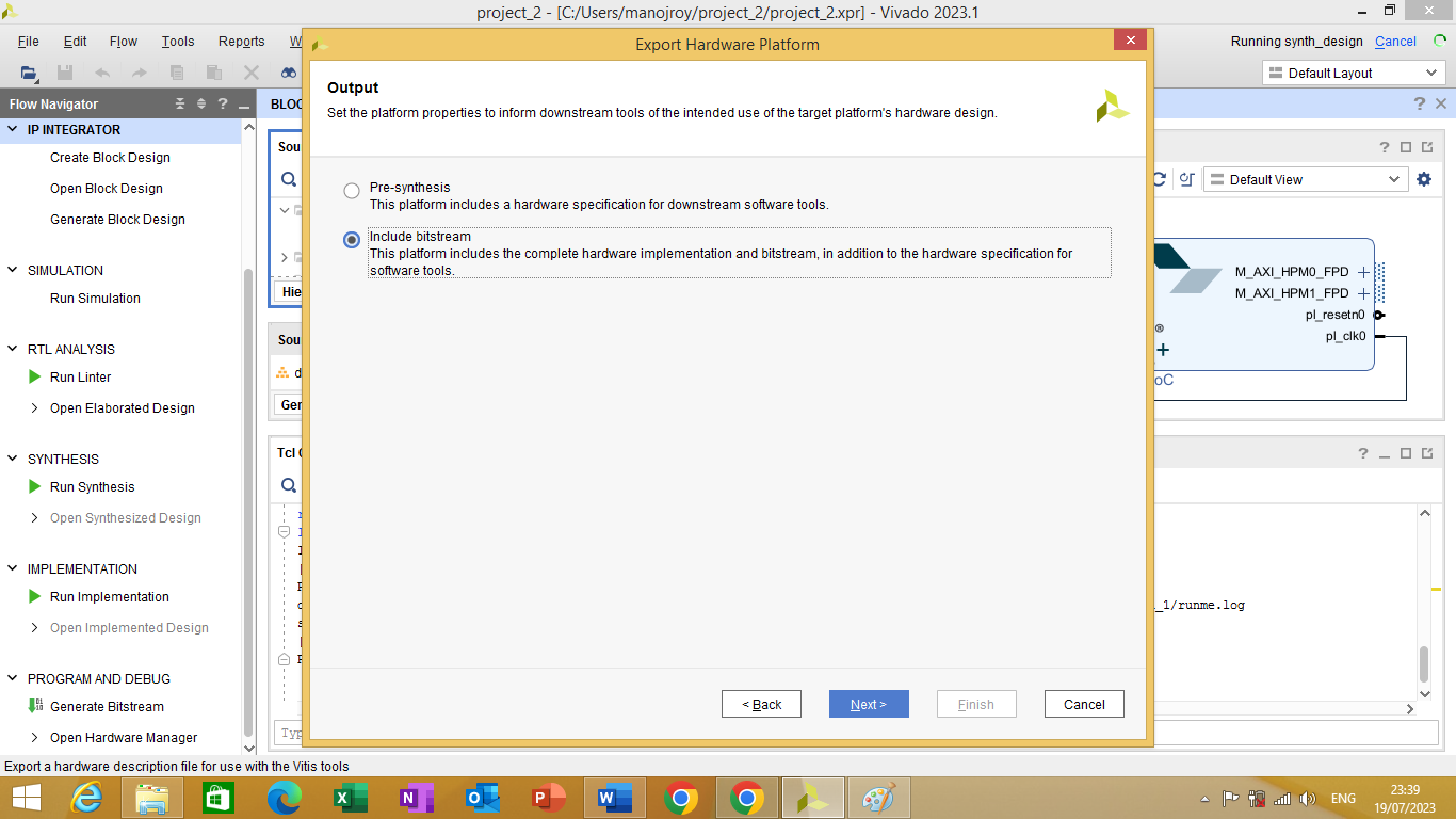
figure 2.17
After that click next. A file window will open as shown in figure 2.18 bellow.
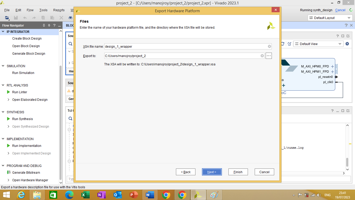
Figure 2.18
Click on finish to complete the setup. Final step is to check where wrapper is stored.
