


The Vivado Design Suite provides an IP-centric design flow that helps us quickly turn designs and algorithms into reusable IPs. The Vivado IP catalog is a unified IP repository that provides the framework for the IP-centric design flow. This catalog consolidates IP from all sources including AMD IP, third-party IP, and end-user designs targeted for reuse as IP into a single environment.
In this blog post, I will create a custom AXI IP block in Vivado and modify its functionality by integrating custom Verilog code. I will be using the Zynq SoC and the MiniZed as a hardware platform. As this is my first IP I will try to keep it very simple. Here I will control some LEDs using switches which will be accessed through register reads and writes over an AXI bus.
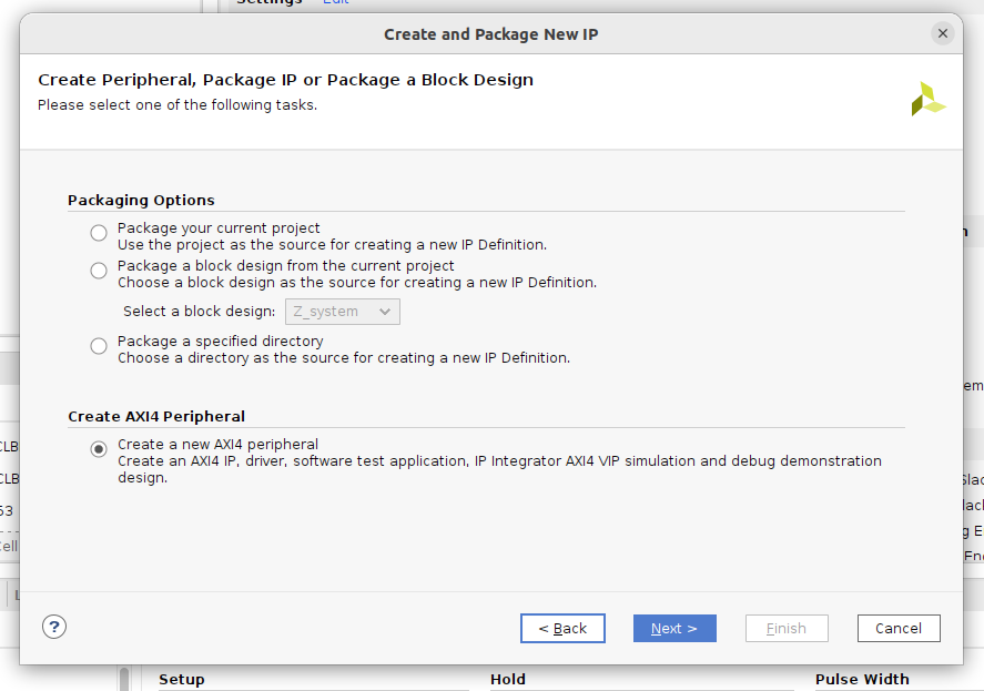
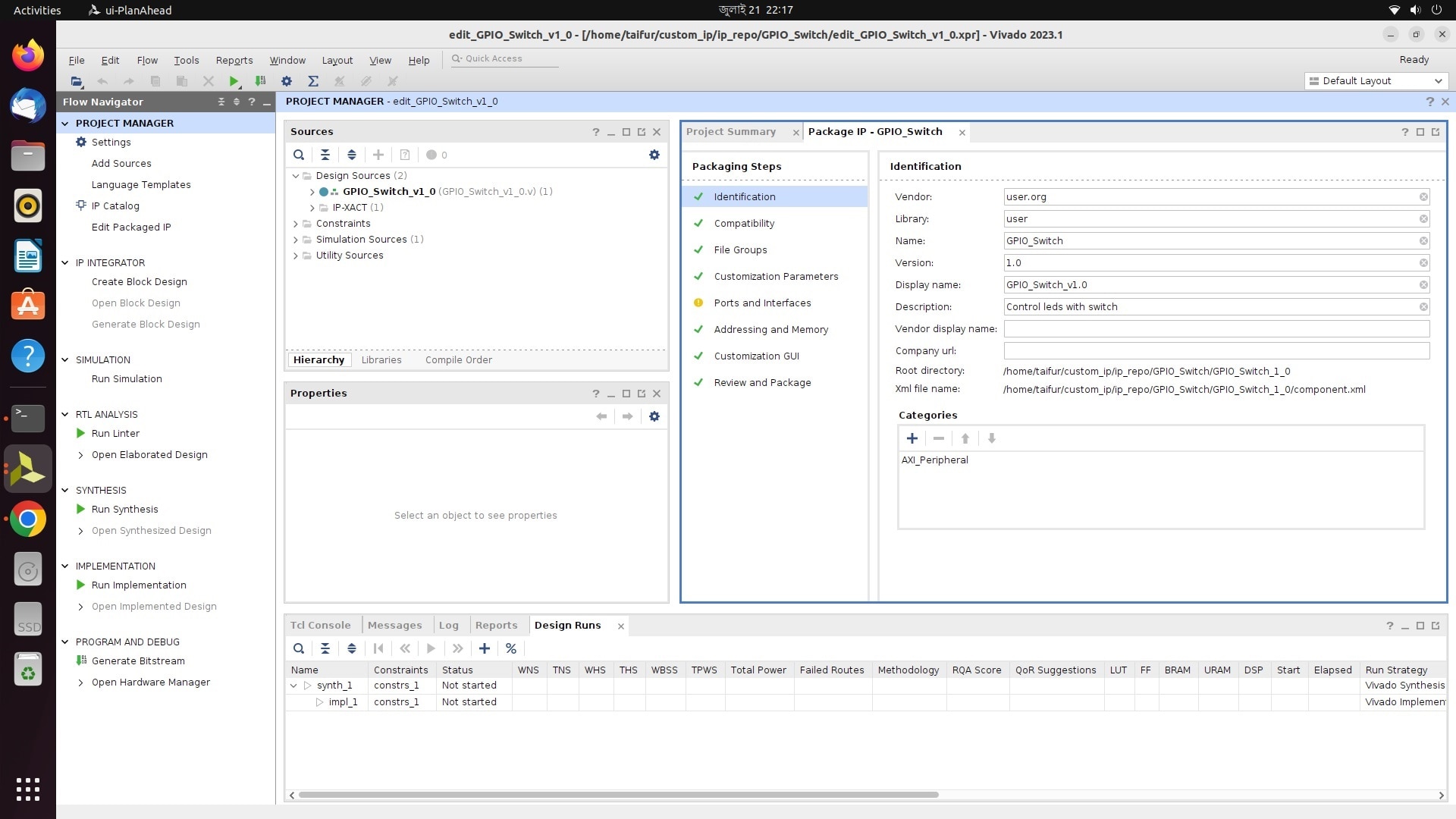
I started to define a new custom IP from an existing AMD Vivado project, using the Create and Package New IP wizard.
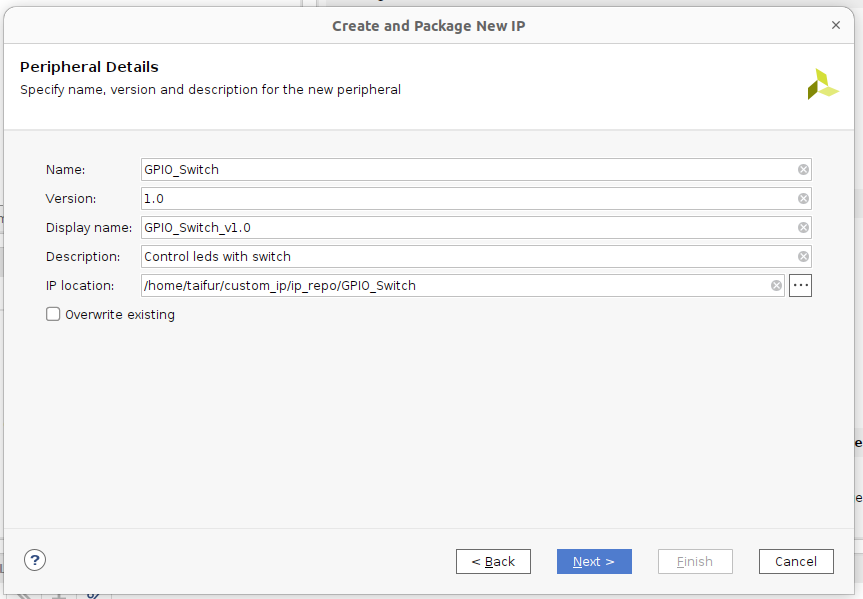
You need to give a name for the IP:
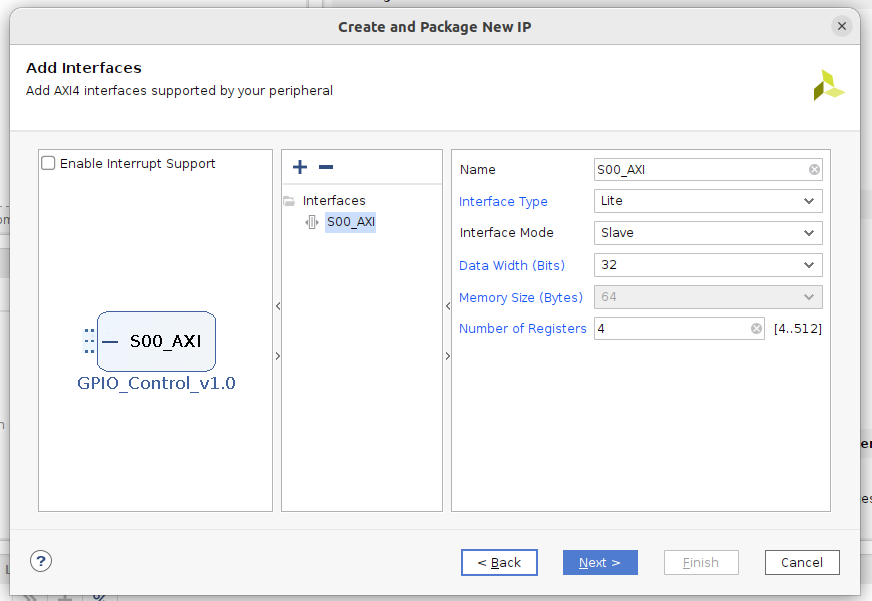
I choose "Create a new AXI4 peripheral". I let all as default from Add Interface window for the AXI interface.
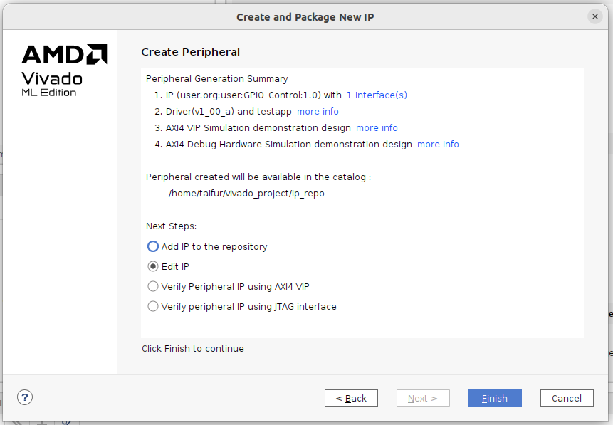
I choose the Edit IP option before clicking on finish button.
After clicking on the finish button Vivado open a new project like below.
I made some modifications on both the Verilog files:
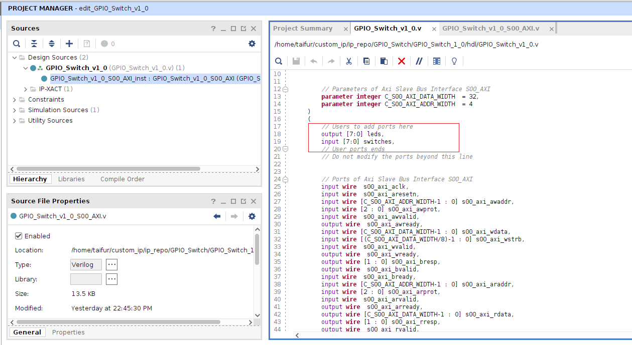
The modified Verilog code for the GPIO_Switch_v1_0.v is as follows:
`timescale 1 ns / 1 ps

	module GPIO_Switch_v1_0 #
	(
		// Users to add parameters here

		// User parameters ends
		// Do not modify the parameters beyond this line


		// Parameters of Axi Slave Bus Interface S00_AXI
		parameter integer C_S00_AXI_DATA_WIDTH	= 32,
		parameter integer C_S00_AXI_ADDR_WIDTH	= 4
	)
	(
		// Users to add ports here
        output [7:0] leds,
        input [7:0] switches,
		// User ports ends
		// Do not modify the ports beyond this line


		// Ports of Axi Slave Bus Interface S00_AXI
		input wire  s00_axi_aclk,
		input wire  s00_axi_aresetn,
		input wire [C_S00_AXI_ADDR_WIDTH-1 : 0] s00_axi_awaddr,
		input wire [2 : 0] s00_axi_awprot,
		input wire  s00_axi_awvalid,
		output wire  s00_axi_awready,
		input wire [C_S00_AXI_DATA_WIDTH-1 : 0] s00_axi_wdata,
		input wire [(C_S00_AXI_DATA_WIDTH/8)-1 : 0] s00_axi_wstrb,
		input wire  s00_axi_wvalid,
		output wire  s00_axi_wready,
		output wire [1 : 0] s00_axi_bresp,
		output wire  s00_axi_bvalid,
		input wire  s00_axi_bready,
		input wire [C_S00_AXI_ADDR_WIDTH-1 : 0] s00_axi_araddr,
		input wire [2 : 0] s00_axi_arprot,
		input wire  s00_axi_arvalid,
		output wire  s00_axi_arready,
		output wire [C_S00_AXI_DATA_WIDTH-1 : 0] s00_axi_rdata,
		output wire [1 : 0] s00_axi_rresp,
		output wire  s00_axi_rvalid,
		input wire  s00_axi_rready
	);
// Instantiation of Axi Bus Interface S00_AXI
	GPIO_Switch_v1_0_S00_AXI # (
		.C_S_AXI_DATA_WIDTH(C_S00_AXI_DATA_WIDTH),
		.C_S_AXI_ADDR_WIDTH(C_S00_AXI_ADDR_WIDTH)
	) GPIO_Switch_v1_0_S00_AXI_inst (
		.S_AXI_ACLK(s00_axi_aclk),
		.S_AXI_ARESETN(s00_axi_aresetn),
		.S_AXI_AWADDR(s00_axi_awaddr),
		.S_AXI_AWPROT(s00_axi_awprot),
		.S_AXI_AWVALID(s00_axi_awvalid),
		.S_AXI_AWREADY(s00_axi_awready),
		.S_AXI_WDATA(s00_axi_wdata),
		.S_AXI_WSTRB(s00_axi_wstrb),
		.S_AXI_WVALID(s00_axi_wvalid),
		.S_AXI_WREADY(s00_axi_wready),
		.S_AXI_BRESP(s00_axi_bresp),
		.S_AXI_BVALID(s00_axi_bvalid),
		.S_AXI_BREADY(s00_axi_bready),
		.S_AXI_ARADDR(s00_axi_araddr),
		.S_AXI_ARPROT(s00_axi_arprot),
		.S_AXI_ARVALID(s00_axi_arvalid),
		.S_AXI_ARREADY(s00_axi_arready),
		.S_AXI_RDATA(s00_axi_rdata),
		.S_AXI_RRESP(s00_axi_rresp),
		.S_AXI_RVALID(s00_axi_rvalid),
		.S_AXI_RREADY(s00_axi_rready),
		.leds(leds),
		.switches(switches)
	);

	// Add user logic here

	// User logic ends

	endmodule
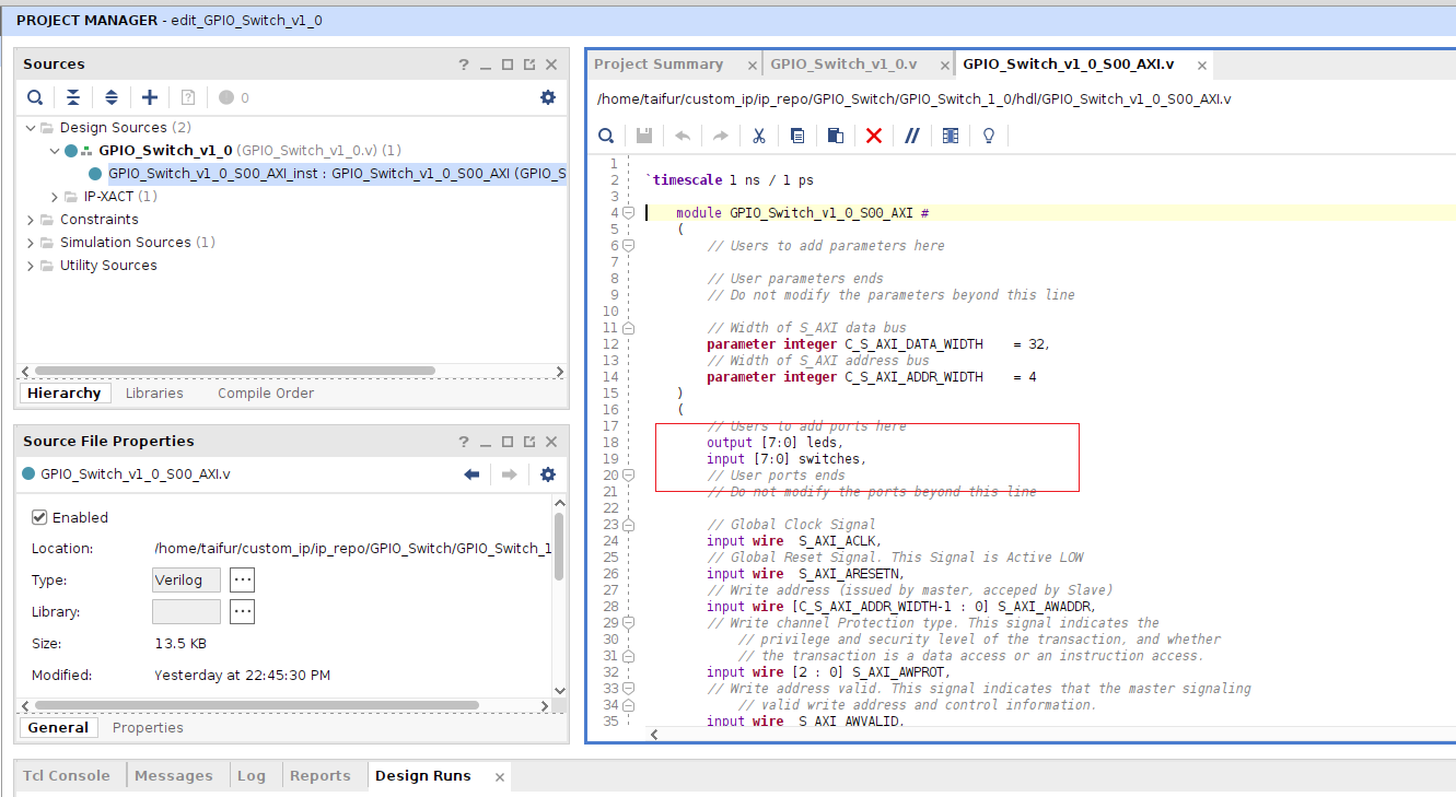
The modified Verilog code for the GPIO_Switch_v1_0_S00_AXI.v is as follows:
`timescale 1 ns / 1 ps

	module GPIO_Switch_v1_0_S00_AXI #
	(
		// Users to add parameters here

		// User parameters ends
		// Do not modify the parameters beyond this line

		// Width of S_AXI data bus
		parameter integer C_S_AXI_DATA_WIDTH	= 32,
		// Width of S_AXI address bus
		parameter integer C_S_AXI_ADDR_WIDTH	= 4
	)
	(
		// Users to add ports here
        output [7:0] leds,
        input [7:0] switches,
		// User ports ends
		// Do not modify the ports beyond this line

		// Global Clock Signal
		input wire  S_AXI_ACLK,
		// Global Reset Signal. This Signal is Active LOW
		input wire  S_AXI_ARESETN,
		// Write address (issued by master, acceped by Slave)
		input wire [C_S_AXI_ADDR_WIDTH-1 : 0] S_AXI_AWADDR,
		// Write channel Protection type. This signal indicates the
    		// privilege and security level of the transaction, and whether
    		// the transaction is a data access or an instruction access.
		input wire [2 : 0] S_AXI_AWPROT,
		// Write address valid. This signal indicates that the master signaling
    		// valid write address and control information.
		input wire  S_AXI_AWVALID,
		// Write address ready. This signal indicates that the slave is ready
    		// to accept an address and associated control signals.
		output wire  S_AXI_AWREADY,
		// Write data (issued by master, acceped by Slave)
		input wire [C_S_AXI_DATA_WIDTH-1 : 0] S_AXI_WDATA,
		// Write strobes. This signal indicates which byte lanes hold
    		// valid data. There is one write strobe bit for each eight
    		// bits of the write data bus.
		input wire [(C_S_AXI_DATA_WIDTH/8)-1 : 0] S_AXI_WSTRB,
		// Write valid. This signal indicates that valid write
    		// data and strobes are available.
		input wire  S_AXI_WVALID,
		// Write ready. This signal indicates that the slave
    		// can accept the write data.
		output wire  S_AXI_WREADY,
		// Write response. This signal indicates the status
    		// of the write transaction.
		output wire [1 : 0] S_AXI_BRESP,
		// Write response valid. This signal indicates that the channel
    		// is signaling a valid write response.
		output wire  S_AXI_BVALID,
		// Response ready. This signal indicates that the master
    		// can accept a write response.
		input wire  S_AXI_BREADY,
		// Read address (issued by master, acceped by Slave)
		input wire [C_S_AXI_ADDR_WIDTH-1 : 0] S_AXI_ARADDR,
		// Protection type. This signal indicates the privilege
    		// and security level of the transaction, and whether the
    		// transaction is a data access or an instruction access.
		input wire [2 : 0] S_AXI_ARPROT,
		// Read address valid. This signal indicates that the channel
    		// is signaling valid read address and control information.
		input wire  S_AXI_ARVALID,
		// Read address ready. This signal indicates that the slave is
    		// ready to accept an address and associated control signals.
		output wire  S_AXI_ARREADY,
		// Read data (issued by slave)
		output wire [C_S_AXI_DATA_WIDTH-1 : 0] S_AXI_RDATA,
		// Read response. This signal indicates the status of the
    		// read transfer.
		output wire [1 : 0] S_AXI_RRESP,
		// Read valid. This signal indicates that the channel is
    		// signaling the required read data.
		output wire  S_AXI_RVALID,
		// Read ready. This signal indicates that the master can
    		// accept the read data and response information.
		input wire  S_AXI_RREADY
	);

	// AXI4LITE signals
	reg [C_S_AXI_ADDR_WIDTH-1 : 0] 	axi_awaddr;
	reg  	axi_awready;
	reg  	axi_wready;
	reg [1 : 0] 	axi_bresp;
	reg  	axi_bvalid;
	reg [C_S_AXI_ADDR_WIDTH-1 : 0] 	axi_araddr;
	reg  	axi_arready;
	reg [C_S_AXI_DATA_WIDTH-1 : 0] 	axi_rdata;
	reg [1 : 0] 	axi_rresp;
	reg  	axi_rvalid;

	// Example-specific design signals
	// local parameter for addressing 32 bit / 64 bit C_S_AXI_DATA_WIDTH
	// ADDR_LSB is used for addressing 32/64 bit registers/memories
	// ADDR_LSB = 2 for 32 bits (n downto 2)
	// ADDR_LSB = 3 for 64 bits (n downto 3)
	localparam integer ADDR_LSB = (C_S_AXI_DATA_WIDTH/32) + 1;
	localparam integer OPT_MEM_ADDR_BITS = 1;
	//----------------------------------------------
	//-- Signals for user logic register space example
	//------------------------------------------------
	//-- Number of Slave Registers 4
	reg [C_S_AXI_DATA_WIDTH-1:0]	slv_reg0;
	reg [C_S_AXI_DATA_WIDTH-1:0]	slv_reg1;
	reg [C_S_AXI_DATA_WIDTH-1:0]	slv_reg2;
	reg [C_S_AXI_DATA_WIDTH-1:0]	slv_reg3;
	wire	 slv_reg_rden;
	wire	 slv_reg_wren;
	reg [C_S_AXI_DATA_WIDTH-1:0]	 reg_data_out;
	integer	 byte_index;
	reg	 aw_en;

	// I/O Connections assignments

	assign leds = slv_reg0;

	assign S_AXI_AWREADY	= axi_awready;
	assign S_AXI_WREADY	= axi_wready;
	assign S_AXI_BRESP	= axi_bresp;
	assign S_AXI_BVALID	= axi_bvalid;
	assign S_AXI_ARREADY	= axi_arready;
	assign S_AXI_RDATA	= axi_rdata;
	assign S_AXI_RRESP	= axi_rresp;
	assign S_AXI_RVALID	= axi_rvalid;
	// Implement axi_awready generation
	// axi_awready is asserted for one S_AXI_ACLK clock cycle when both
	// S_AXI_AWVALID and S_AXI_WVALID are asserted. axi_awready is
	// de-asserted when reset is low.

	always @( posedge S_AXI_ACLK )
	begin
	  if ( S_AXI_ARESETN == 1'b0 )
	    begin
	      axi_awready <= 1'b0;
	      aw_en <= 1'b1;
	    end
	  else
	    begin
	      if (~axi_awready && S_AXI_AWVALID && S_AXI_WVALID && aw_en)
	        begin
	          // slave is ready to accept write address when
	          // there is a valid write address and write data
	          // on the write address and data bus. This design
	          // expects no outstanding transactions.
	          axi_awready <= 1'b1;
	          aw_en <= 1'b0;
	        end
	        else if (S_AXI_BREADY && axi_bvalid)
	            begin
	              aw_en <= 1'b1;
	              axi_awready <= 1'b0;
	            end
	      else
	        begin
	          axi_awready <= 1'b0;
	        end
	    end
	end

	// Implement axi_awaddr latching
	// This process is used to latch the address when both
	// S_AXI_AWVALID and S_AXI_WVALID are valid.

	always @( posedge S_AXI_ACLK )
	begin
	  if ( S_AXI_ARESETN == 1'b0 )
	    begin
	      axi_awaddr <= 0;
	    end
	  else
	    begin
	      if (~axi_awready && S_AXI_AWVALID && S_AXI_WVALID && aw_en)
	        begin
	          // Write Address latching
	          axi_awaddr <= S_AXI_AWADDR;
	        end
	    end
	end

	// Implement axi_wready generation
	// axi_wready is asserted for one S_AXI_ACLK clock cycle when both
	// S_AXI_AWVALID and S_AXI_WVALID are asserted. axi_wready is
	// de-asserted when reset is low.

	always @( posedge S_AXI_ACLK )
	begin
	  if ( S_AXI_ARESETN == 1'b0 )
	    begin
	      axi_wready <= 1'b0;
	    end
	  else
	    begin
	      if (~axi_wready && S_AXI_WVALID && S_AXI_AWVALID && aw_en )
	        begin
	          // slave is ready to accept write data when
	          // there is a valid write address and write data
	          // on the write address and data bus. This design
	          // expects no outstanding transactions.
	          axi_wready <= 1'b1;
	        end
	      else
	        begin
	          axi_wready <= 1'b0;
	        end
	    end
	end

	// Implement memory mapped register select and write logic generation
	// The write data is accepted and written to memory mapped registers when
	// axi_awready, S_AXI_WVALID, axi_wready and S_AXI_WVALID are asserted. Write strobes are used to
	// select byte enables of slave registers while writing.
	// These registers are cleared when reset (active low) is applied.
	// Slave register write enable is asserted when valid address and data are available
	// and the slave is ready to accept the write address and write data.
	assign slv_reg_wren = axi_wready && S_AXI_WVALID && axi_awready && S_AXI_AWVALID;

	always @( posedge S_AXI_ACLK )
	begin
	  if ( S_AXI_ARESETN == 1'b0 )
	    begin
	      slv_reg0 <= 0;
	      slv_reg2 <= 0;
	      slv_reg3 <= 0;
	    end
	  else begin

	    if (slv_reg_wren)
	      begin
	        case ( axi_awaddr[ADDR_LSB+OPT_MEM_ADDR_BITS:ADDR_LSB] )
	          2'h0:
	            for ( byte_index = 0; byte_index <= (C_S_AXI_DATA_WIDTH/8)-1; byte_index = byte_index+1 )
	              if ( S_AXI_WSTRB[byte_index] == 1 ) begin
	                // Respective byte enables are asserted as per write strobes
	                // Slave register 0
	                slv_reg0[(byte_index*8) +: 8] <= S_AXI_WDATA[(byte_index*8) +: 8];
	              end
	          2'h2:
	            for ( byte_index = 0; byte_index <= (C_S_AXI_DATA_WIDTH/8)-1; byte_index = byte_index+1 )
	              if ( S_AXI_WSTRB[byte_index] == 1 ) begin
	                // Respective byte enables are asserted as per write strobes
	                // Slave register 2
	                slv_reg2[(byte_index*8) +: 8] <= S_AXI_WDATA[(byte_index*8) +: 8];
	              end
	          2'h3:
	            for ( byte_index = 0; byte_index <= (C_S_AXI_DATA_WIDTH/8)-1; byte_index = byte_index+1 )
	              if ( S_AXI_WSTRB[byte_index] == 1 ) begin
	                // Respective byte enables are asserted as per write strobes
	                // Slave register 3
	                slv_reg3[(byte_index*8) +: 8] <= S_AXI_WDATA[(byte_index*8) +: 8];
	              end
	          default : begin
	                      slv_reg0 <= slv_reg0;
	                      slv_reg2 <= slv_reg2;
	                      slv_reg3 <= slv_reg3;
	                    end
	        endcase
	      end
	  end
	end

    always @( posedge S_AXI_ACLK )
	begin
	  if ( S_AXI_ARESETN == 1'b0 )
	  begin
		slv_reg1 <= 0;
	  end
	  else
	  begin
	    slv_reg1 <= switches;
	  end
    end

	// Implement write response logic generation
	// The write response and response valid signals are asserted by the slave
	// when axi_wready, S_AXI_WVALID, axi_wready and S_AXI_WVALID are asserted.
	// This marks the acceptance of address and indicates the status of
	// write transaction.

	always @( posedge S_AXI_ACLK )
	begin
	  if ( S_AXI_ARESETN == 1'b0 )
	    begin
	      axi_bvalid  <= 0;
	      axi_bresp   <= 2'b0;
	    end
	  else
	    begin
	      if (axi_awready && S_AXI_AWVALID && ~axi_bvalid && axi_wready && S_AXI_WVALID)
	        begin
	          // indicates a valid write response is available
	          axi_bvalid <= 1'b1;
	          axi_bresp  <= 2'b0; // 'OKAY' response
	        end                   // work error responses in future
	      else
	        begin
	          if (S_AXI_BREADY && axi_bvalid)
	            //check if bready is asserted while bvalid is high)
	            //(there is a possibility that bready is always asserted high)
	            begin
	              axi_bvalid <= 1'b0;
	            end
	        end
	    end
	end

	// Implement axi_arready generation
	// axi_arready is asserted for one S_AXI_ACLK clock cycle when
	// S_AXI_ARVALID is asserted. axi_awready is
	// de-asserted when reset (active low) is asserted.
	// The read address is also latched when S_AXI_ARVALID is
	// asserted. axi_araddr is reset to zero on reset assertion.

	always @( posedge S_AXI_ACLK )
	begin
	  if ( S_AXI_ARESETN == 1'b0 )
	    begin
	      axi_arready <= 1'b0;
	      axi_araddr  <= 32'b0;
	    end
	  else
	    begin
	      if (~axi_arready && S_AXI_ARVALID)
	        begin
	          // indicates that the slave has acceped the valid read address
	          axi_arready <= 1'b1;
	          // Read address latching
	          axi_araddr  <= S_AXI_ARADDR;
	        end
	      else
	        begin
	          axi_arready <= 1'b0;
	        end
	    end
	end

	// Implement axi_arvalid generation
	// axi_rvalid is asserted for one S_AXI_ACLK clock cycle when both
	// S_AXI_ARVALID and axi_arready are asserted. The slave registers
	// data are available on the axi_rdata bus at this instance. The
	// assertion of axi_rvalid marks the validity of read data on the
	// bus and axi_rresp indicates the status of read transaction.axi_rvalid
	// is deasserted on reset (active low). axi_rresp and axi_rdata are
	// cleared to zero on reset (active low).
	always @( posedge S_AXI_ACLK )
	begin
	  if ( S_AXI_ARESETN == 1'b0 )
	    begin
	      axi_rvalid <= 0;
	      axi_rresp  <= 0;
	    end
	  else
	    begin
	      if (axi_arready && S_AXI_ARVALID && ~axi_rvalid)
	        begin
	          // Valid read data is available at the read data bus
	          axi_rvalid <= 1'b1;
	          axi_rresp  <= 2'b0; // 'OKAY' response
	        end
	      else if (axi_rvalid && S_AXI_RREADY)
	        begin
	          // Read data is accepted by the master
	          axi_rvalid <= 1'b0;
	        end
	    end
	end

	// Implement memory mapped register select and read logic generation
	// Slave register read enable is asserted when valid address is available
	// and the slave is ready to accept the read address.
	assign slv_reg_rden = axi_arready & S_AXI_ARVALID & ~axi_rvalid;
	always @(*)
	begin
	      // Address decoding for reading registers
	      case ( axi_araddr[ADDR_LSB+OPT_MEM_ADDR_BITS:ADDR_LSB] )
	        2'h0   : reg_data_out <= slv_reg0;
	        2'h1   : reg_data_out <= slv_reg1;
	        2'h2   : reg_data_out <= slv_reg2;
	        2'h3   : reg_data_out <= slv_reg3;
	        default : reg_data_out <= 0;
	      endcase
	end

	// Output register or memory read data
	always @( posedge S_AXI_ACLK )
	begin
	  if ( S_AXI_ARESETN == 1'b0 )
	    begin
	      axi_rdata  <= 0;
	    end
	  else
	    begin
	      // When there is a valid read address (S_AXI_ARVALID) with
	      // acceptance of read address by the slave (axi_arready),
	      // output the read dada
	      if (slv_reg_rden)
	        begin
	          axi_rdata <= reg_data_out;     // register read data
	        end
	    end
	end

	// Add user logic here

	// User logic ends

	endmodule
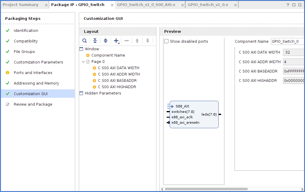
The customized IP block GUI will look as follows:
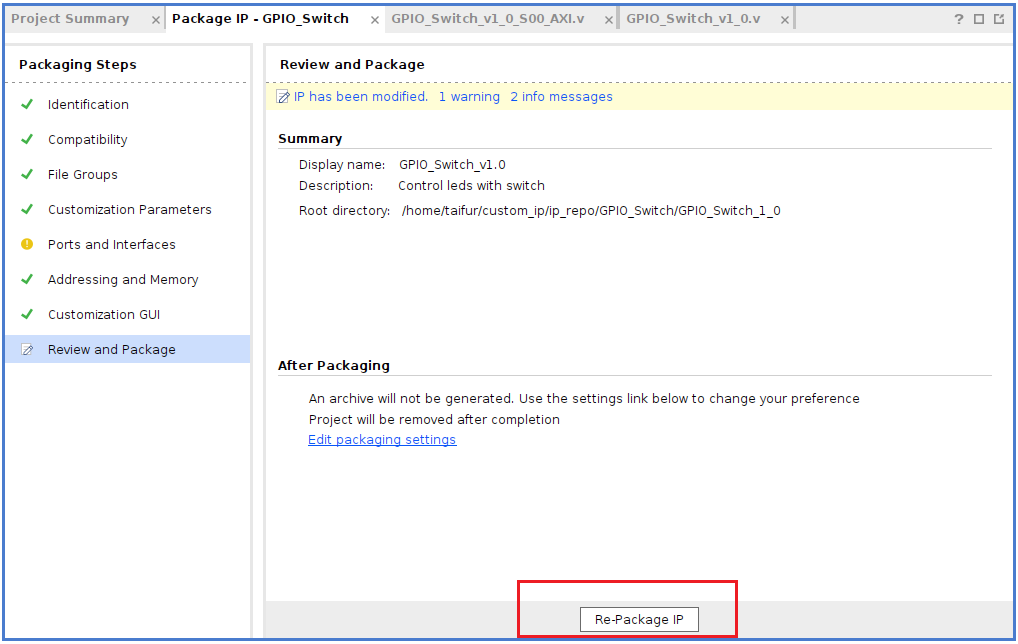
As we have modified the Verilog code we need to Re-Package the IP.
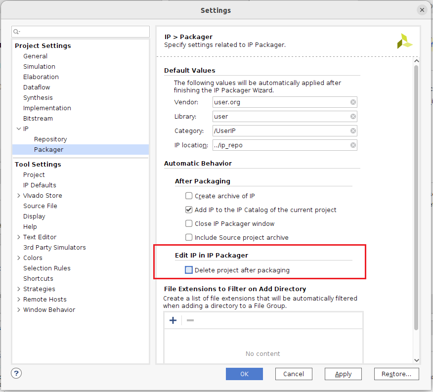
Before Applying the changes I unchecked the following check box marked as red.
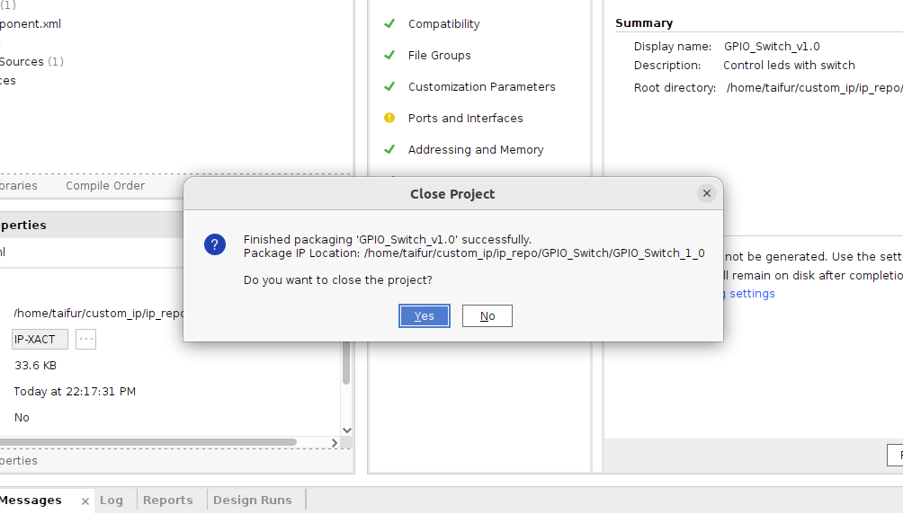
After finishing our customized IP is ready and we may close the project.
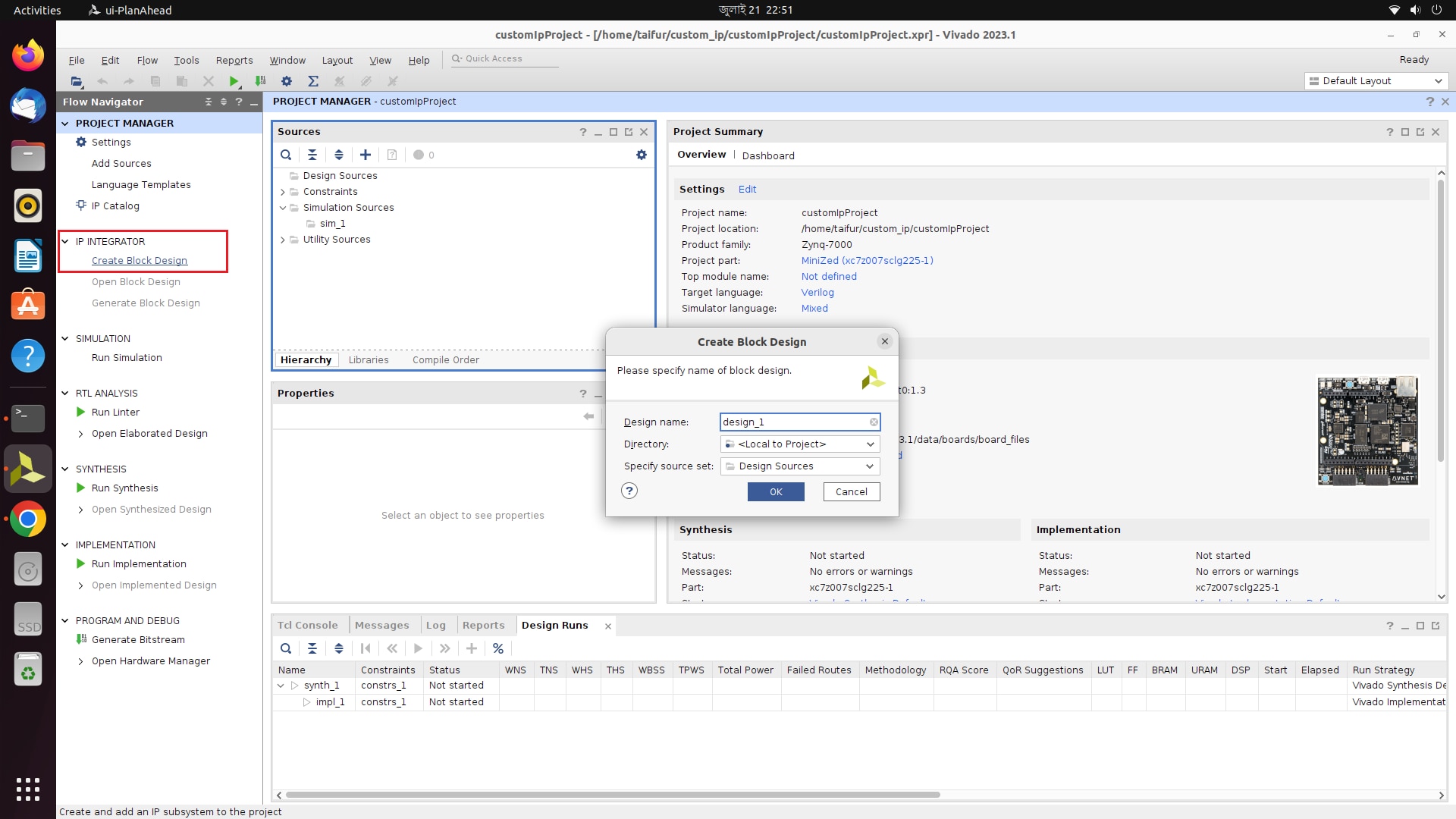
Now we are in our original project environment and I am going to add the customized IP block I just created in my project with the ZYNQ processing block.
Using the Create Block Design option in the Flow Navigator window, I added a new block design to the project.
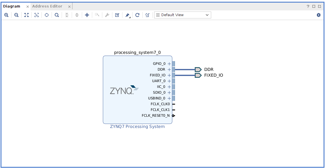
Add the Zynq processing system IP block to the design and run the Block Automation that appears to apply the board presets and other basic/bare bones settings to it.
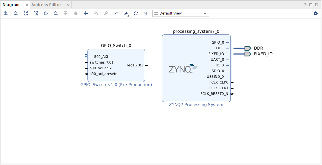
To add the customized IP block that we created in the previous step, right-click anywhere in the blank space of the Diagram window and select the Add IP... option. Search for the GPIO_Switch and add the IP to the block design.
Then I added the AXI Interconnect IP to the design and run the automation again.
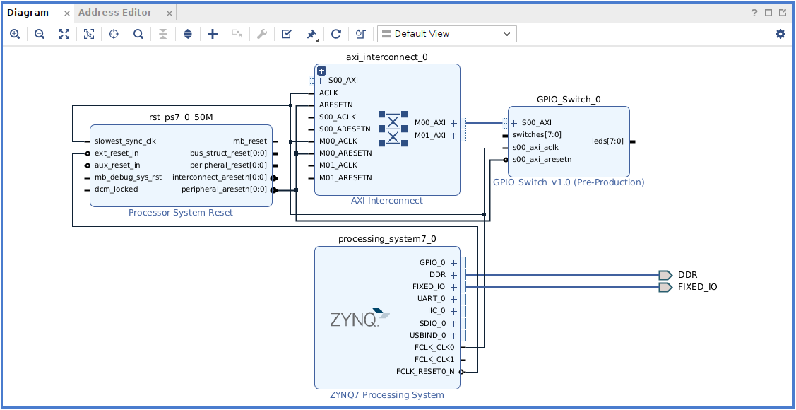
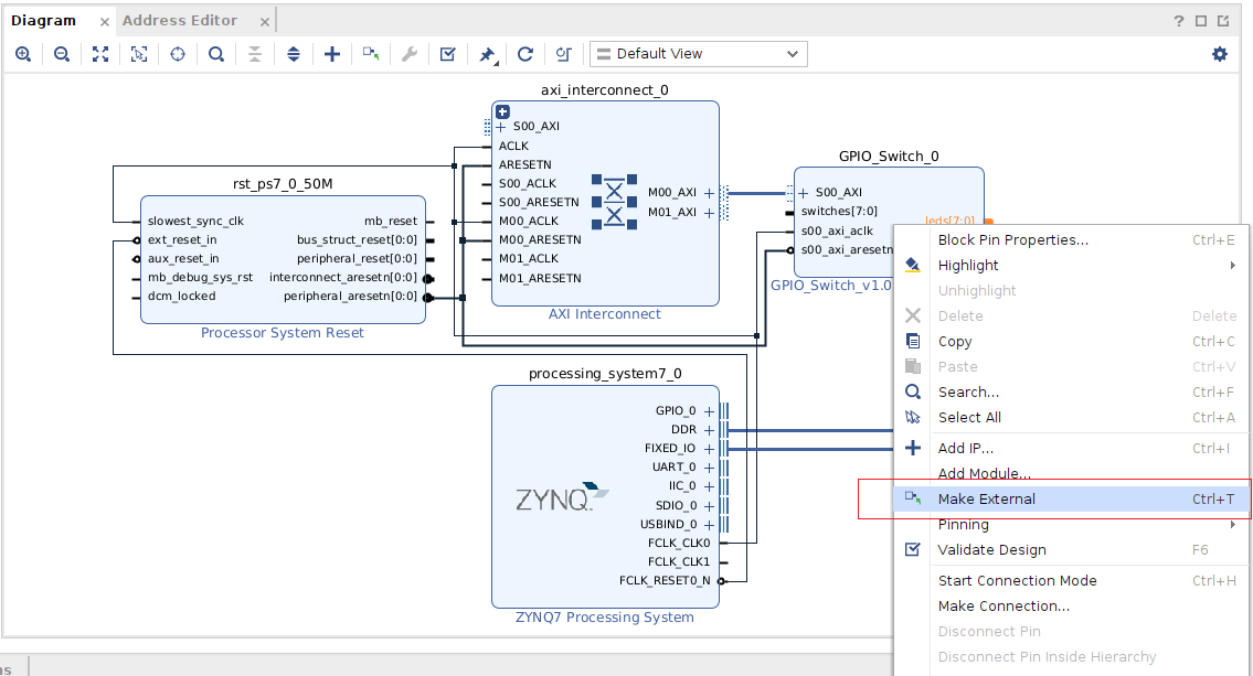
I made the LEDs and switches terminal of the custom IP block external.
After connecting all the terminals the block looks like as below:
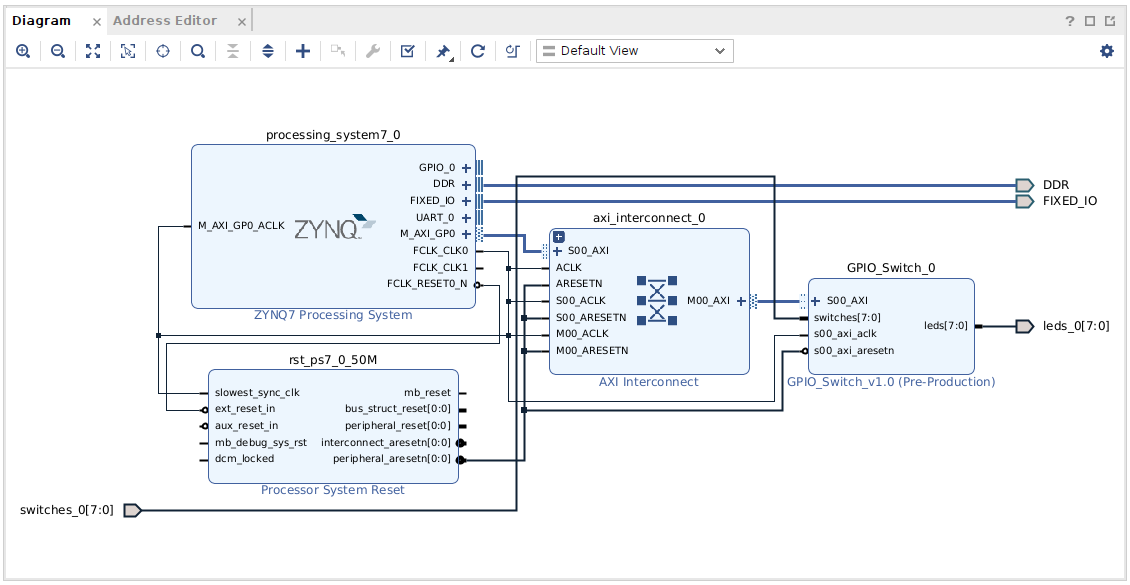
After getting it all connected, the design successfully passed validation with one minor warning about ensuring the clock property was synced with the custom module, but this warning can be safely ignored.
With the block design complete, a HDL wrapper can be generated for the design and left to Vivado to auto-manage:
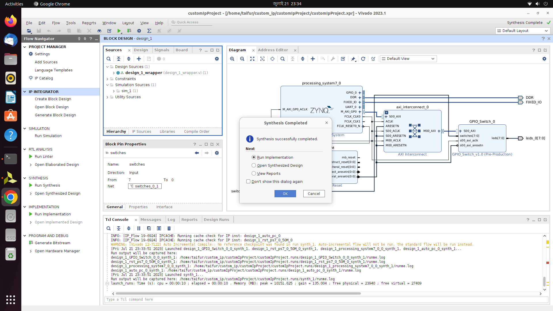
Finally, I run the Synthesis, and the synthesis was successfully completed as there is no error in the block design.
-

javagoza
-
Cancel
-
Vote Up
0
Vote Down
-
-
Sign in to reply
-
More
-
Cancel
-

taifur
in reply to javagoza
-
Cancel
-
Vote Up
0
Vote Down
-
-
Sign in to reply
-
More
-
Cancel
Comment-

taifur
in reply to javagoza
-
Cancel
-
Vote Up
0
Vote Down
-
-
Sign in to reply
-
More
-
Cancel
Children