


In this tutorial we will learn how to create a custom AXI4 Lite IP Peripheral implementing a tachometer. We will add two quadrature encoders with Hall effect sensors to the mini plastic gear motors of the ArtyBot. The tachometer will enable the robot to measure motor rotational speed. With the tachometer data we will be able to drive the ArtyBot straight, drive it for a prescribed amount of distance or turn it at a prescribed angle.
This tutorial post is part 5 of my contribution to the "7 Ways to Leave Your Spartan-6" program, learning about the Xilinx Spartan-7 FPGA on the Digilent Arty S7 50 board.
Based on the libraries for the Digilent Pmod DHB1 module, we are going to replicate the operation of the DC motor feedback module, reviewing the process from the design of a custom RTL module in Verilog HDL language, to the creation of an AXI4-Lite Interface Wrapper for use in the Vivado IP Integrator. And finally creating a software driver in C-language to interact with our module and be able to calculate speeds and relative positions of the Artybot.
In the following video you can see the operation of the module. Displaying speed and position data in real time with a PmodOLED
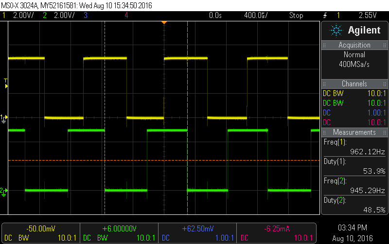
Hall sensors output simulated with the Analog Discovery 2 Waveform Generator by two pulse signals sweeping from 1 Hz to 200Hz in 20 s for one motor and from 1Hz to 500Hz in 20s for the other motor.
Tutorial Environment
For this tutorial you'll need, Windows 10, AMD Xilinx Vivado ML 2021.1 and the following hardware:
| Product Name | Manufacturer | Datasheet |
| Arty S7 50 | Digilent | Buy Now |
| TI-RSLK | element14 | Buy Now |
Also we'll use a Logic Analyzer and the Waveform generator from the Digilent Analog Discovery 2 USB Oscilloscope
The sensors
We will use the Pololu - Romi Encoder Pair Kit. These quadrature encoders use a magnetic disc and Hall effect sensors to provide 12 counts per revolution of the motor shaft.
| {gallery}Pololu - Romi Encoder Pair Kit. |
|---|
|
Romi Encoder Pair Kit |
|
Encoder A and B outputs of a magnetic encoder on a high-power (HP) mini plastic gearmotor running at 4.5 V |

The sensors operate from 3.5 V to 18 V and provide digital outputs. The outputs (ELA, ELB, ERA, ERB) are pull up to VPU 3V3 from the Arty S7 board.

For our calculations we also need the reduction ratio of our DC motors gearbox. We are using two high-power brushed DC motor with a 120:1 reduction gearbox. Exact gear ratio:

Also we will need the wheels diameter that is 70 mm for our model.
References: Pololu - Romi Encoder Pair Kit, 12 CPR, 3.5-18V, Pololu - 120:1 Mini Plastic Gearmotor HP, Offset 3mm D-Shaft Output, Extended Motor Shaft, Pololu Wheel 70×8mm Pair - White
Control System and Tachometer
We want to build a control system for our robot. With a control system, we can independently set the rotation speed of each motor. The control system measures speed and uses feedback to adjust the PWM duty cycle of each motor to achieve the desired speed. With the control system, the robot can move in a straight line, run at a desired speed, travel a prescribed distance, or turn at a prescribed angle.
A tachometer is a sensor with digital outputs that relate to rotational speed.
The motors used on the Romi have a 120:1 gear reduction and the encoders are connected directly to the motor output shaft and have 12 Counts Per Revolution (CPR). With the provided gear ratio, this nets 1440 counts per wheel revolution. We will use only one sensor output and will count only rising edges so each output pulses 360 times per rotation. If we measure the Period (in sec) of one of the tachometer signals, we can calculate the motor Speed in rpm as
Speed = 360*60/Period
Verilog HDL Modules
Differential Motors Position Module.
We will start designing our top module. Our top module will be a Differential Motors Position Module.
This module that will allow us to:
- Get Speeds : Measure current angular speeds of motor1 and motor2 (in RPM) and store them in motor speed.
- Get Distance Traveled: Return mean distance traveled by motor1 and motor2
- Get Edge Counts: Get sensor and clock edge counts of each motor for computing speed
- Clear Speed Counters: Clear the registers storing counts of sensor and clock edges for computing speed
- Get Motor Positions: Get current positions of the two motors
- Get Position Difference: Get current position difference between motor1 and motor2
- Clear Position Counters: Clear the cumulative position counters for both motors
Several counters are needed, two for control position and another two for speed calculation.
The design of the FPGA will allow us to increment the counters in parallel and not lose any increments and also get the difference of two counters at the same time.
The module has three inputs. Two inputs for the motor sensors and another input to clear the control counters.

Inputs
- clk: Clock
- hallSensorM1: Sensor input signal from the encoder of motor 1
- hallSensorM2: Sensor input signal from the encoder of motor 2
- clearPosition: Signal for resetting position counters, controlPosition1 and/or controlPosition2
Outputs
- speedPosition1: Counter for speed calculation relative to the motor1
- controlPosition1 : Counter for position control relative to the motor1
- speedPosition2: Counter for speed calculation relative to the motor2
- controlPosition2: Counter for position control relative to the motor1
- differentialPosition: position difference between motor1 and motor2
- clockCounter: Clock pulse counter.
This module will use two Motor Position Counter modules to keep track of the individual counters of each motor.
Motor Position Counter Module
For each DC motor we have a separate module that keeps track of the counters.
It keeps track of two counters, one for position calculation and one for velocity calculation.

Inputs
- clk: clock
- hallSensor: hall sensor input signal
- clearPosition: clearPosition[0] clears position1, // clearPosition[2] clears position2
- subtractDistance: substract distance from controlPosition
- distance: distance amount to subtract from controlPosition
Outputs
- speedPosition: for speed calculation
- controlPosition: for position control
Differential Motors Position Verilog Module
We will use one of the inputs of each encoder to measure the period. We will use counters that are 16 bits wide, so the period measurement will be accurate to 16 bits.
File: differentialMotorPosition.v
`timescale 1ns / 1ps
//////////////////////////////////////////////////////////////////////////////////
// Company:
// Engineer: Enrique Albertos
//
// Create Date: 06/24/2022 09:53:53 PM
// Design Name:
// Module Name: differentialMotorPosition
// Project Name: ArtyBot
// Target Devices: Arty S7 50
// Tool Versions: Vivado 2021.1 ML
// Description: It counts the pulses from two hall sensors in the encoders of
// two motors and calculates the difference between them.
// It allows calculating the angular speed of the two motors
// and the relative position between the two motors.
//
// Dependencies: motorPositionCounter.v
//
// Revision:
// Revision 0.01 - File Created
// Additional Comments:
//
//////////////////////////////////////////////////////////////////////////////////


module differentialMotorPosition (
   input  wire        clk,
   output wire [15:0] speedPosition1,
   output wire [15:0] controlPosition1,
   output wire [15:0] speedPosition2,
   output wire [15:0] controlPosition2,
   output wire [15:0] differentialPosition,
   output reg  [31:0] clockCounter,
   input  wire        hallSensorM1,
   input  wire        hallSensorM2,
   input  wire [1:0]  clearPosition
);
   // delayed signals
   reg hallSensorM1Delay;
   reg hallSensorM2Delay;

   // adjusted signals
   reg hallSensorM1Delayed;
   reg hallSensorM2Delayed;

   initial begin
      clockCounter           = 32'b0;
      hallSensorM1Delay     =  1'b0;
      hallSensorM2Delay     =  1'b0;
      hallSensorM1Delayed  =  1'b0;
      hallSensorM2Delayed  =  1'b0;
   end

   always @ (posedge clk) begin
      if (clearPosition[0]) begin
         clockCounter <= 32'b0;
      end else begin
          clockCounter <= clockCounter + 1'b1;
      end
      // Create delay
      hallSensorM1Delay <= hallSensorM1;
      hallSensorM2Delay <= hallSensorM2;
      hallSensorM1Delayed <= hallSensorM1Delay;
      hallSensorM2Delayed <= hallSensorM2Delay;
   end

   wire subtract;
   assign subtract = controlPosition1[15] | controlPosition2[15];

   reg [15:0] distance;
   always @ (*) begin
      if (controlPosition1 < controlPosition2) begin
          distance = controlPosition1;
      end else begin
          distance = controlPosition2;
      end
   end

   assign differentialPosition = controlPosition1 - controlPosition2;

   motorPositionCounter motorPositionCounter1 (
      .clk(clk),
      .hallSensor(hallSensorM1Delayed),
      .clearPosition(clearPosition),
      .subtractDistance(subtract),
      .distance(distance),
      .speedPosition(speedPosition1),
      .controlPosition(controlPosition1)
   );

   motorPositionCounter motorPositionCounter2 (
      .clk(clk),
      .hallSensor(hallSensorM2Delayed),
      .clearPosition(clearPosition),
      .subtractDistance(subtract),
      .distance(distance),
      .speedPosition(speedPosition2),
      .controlPosition(controlPosition2)
   );
endmodule
Test Bench for the Differential Motors Position Verilog Module
We will use this test bench for simulation. See in the simulation section below the simulation and graph with the Vivado Wave window.
File: differentialMotorPositionTest.v
`timescale 1ns / 1ps
//////////////////////////////////////////////////////////////////////////////////
// Company:
// Engineer: Enrique Albertos
//
// Create Date: 06/25/2022 11:11:15 AM
// Design Name:
// Module Name: differentialMotorPositionTest
// Project Name: ArtyBot
// Target Devices: DUT differentialMotorPosition
// Tool Versions:
// Description:
//
// Dependencies:
//
// Revision:
// Revision 0.01 - File Created
// Additional Comments:
//
//////////////////////////////////////////////////////////////////////////////////


module differentialMotorPositionTest ();
   reg         clk;
   wire [15:0] speedPosition1;
   wire [15:0] controlPosition1;
   wire [15:0] speedPosition2;
   wire [15:0] controlPosition2;
   wire [15:0] differentialPosition;
   wire [31:0] clockCounter;
   reg         hallSensorM1, hallSensorM2;
   reg  [1:0]  clearPosition;

   differentialMotorPosition dut (
      .clk(clk),
      .speedPosition1(speedPosition1),
      .controlPosition1(controlPosition1),
      .speedPosition2(speedPosition2),
      .controlPosition2(controlPosition2),
      .differentialPosition(differentialPosition),
      .clockCounter(clockCounter),
      .hallSensorM1(hallSensorM1),
      .hallSensorM2(hallSensorM2),
      .clearPosition(clearPosition)
   );

   parameter CLOCK_PERIOD = 10;
   initial begin
      clk <= 0;
      forever #(CLOCK_PERIOD / 2) clk <= ~clk;
   end

   integer i;
   initial begin
         hallSensorM1 <= 0; hallSensorM2 <= 0; clearPosition <= 2'b00; @(posedge clk);
         clearPosition <= 2'b01;                                       @(posedge clk);
         clearPosition <= 2'b00;                                       @(posedge clk);
         hallSensorM1 <= 1;                                            @(posedge clk);
         hallSensorM1 <= 0;                                            @(posedge clk);
         hallSensorM1 <= 1;                                            @(posedge clk);
         hallSensorM1 <= 0;                                            @(posedge clk);
         hallSensorM1 <= 1;                                            @(posedge clk);
         hallSensorM1 <= 0;                                            @(posedge clk);
      for (i = 0; i < 16; i = i + 1) begin
         hallSensorM1 <= 0; hallSensorM2 <= 0;                         @(posedge clk);
         hallSensorM1 <= 1; hallSensorM2 <= 1;                         @(posedge clk);
      end
      clearPosition <= 2'b01;                                          @(posedge clk);
      clearPosition <= 2'b00;                                          @(posedge clk);
      for (i = 0; i < 32768; i = i + 1) begin
         hallSensorM1 <= 0; hallSensorM2 <= 0;                         @(posedge clk);
         hallSensorM1 <= 1; hallSensorM2 <= 1;                         @(posedge clk);
      end
      clearPosition <= 2'b10;                                          @(posedge clk);
      clearPosition <= 2'b00;                                          @(posedge clk);
                                                                       @(posedge clk);
                                                                       @(posedge clk);
                                                                       @(posedge clk);
      for (i = 0; i < 16; i = i + 1) begin
         hallSensorM1 <= 0; hallSensorM2 <= 0;                         @(posedge clk);
         hallSensorM1 <= 1; hallSensorM2 <= 1;                         @(posedge clk);
      end
      clearPosition <= 2'b11;                                          @(posedge clk);
      clearPosition <= 2'b00;                                          @(posedge clk);
      hallSensorM2 <= 0;                                               @(posedge clk);
      hallSensorM2 <= 1;                                               @(posedge clk);
      hallSensorM2 <= 0;                                               @(posedge clk);
      hallSensorM2 <= 1;                                               @(posedge clk);
      hallSensorM2 <= 0;                                               @(posedge clk);
      hallSensorM2 <= 1;                                               @(posedge clk);
      hallSensorM2 <= 0;                                               @(posedge clk);
      hallSensorM2 <= 1;                                               @(posedge clk);
      hallSensorM2 <= 0;                                               @(posedge clk);
      hallSensorM2 <= 1;                                               @(posedge clk);
      $stop;
   end
endmodule
Motor Position Counter Verilog Module
motorPositionCounter.v
`timescale 1ns / 1ps
//////////////////////////////////////////////////////////////////////////////////
// Company:
// Engineer: Enrique Albertos
// File: motorPositionCounter.v
// Create Date: 06/24/2022 07:43:14 PM
// Design Name:
// Module Name: motorPositionCounter
// Project Name: ArtyBot
// Target Devices: Arty S7 50
// Tool Versions: Vivado 2021.1
// Description: Motor Position Counter.
// Keeps two counters:
// one for motor speed calculation and another for motor position control
// Dependencies:
//
// Revision:
// Revision 0.01 - File Created
// Additional Comments:
//
//////////////////////////////////////////////////////////////////////////////////


module motorPositionCounter(
    input   wire         clk,                // clock
    input   wire         hallSensor,         // hall sensor input signal
    input   wire  [1:0]  clearPosition,      // clearPosition[0] clears position1,  // clearPosition[2] clears position2
    input   wire         subtractDistance,   // substract distance from controlPosition
    input   wire [15:0]  distance,           // distance amount to subtract from controlPosition
    output  reg  [15:0]  speedPosition,      // for speed calculation
    output  reg  [15:0]  controlPosition     // for position control

    );

    parameter SPEED_POSITION = 0;
    parameter CONTROL_POSITION = 1;

    reg hallSensorOld;

    initial begin
        hallSensorOld   =  1'b0;
        speedPosition   = 16'b0;
        controlPosition = 16'b0;
    end

    always @ (posedge clk) begin
        if (clearPosition[CONTROL_POSITION] | clearPosition[SPEED_POSITION]) begin
            if (clearPosition[SPEED_POSITION] ) begin
                speedPosition <= 16'b0;
             end
             if (clearPosition[CONTROL_POSITION]) begin
                controlPosition <= 16'b0;
             end
        end else if (subtractDistance) begin
            controlPosition <= controlPosition - distance;
        end else if (~hallSensorOld & hallSensor) begin
            speedPosition <= speedPosition + 1'b1;
            controlPosition <= controlPosition + 1'b1;
        end
        // store hallSensor previous state
        hallSensorOld <= hallSensor;
    end
endmodule
Test Bench for the Differential Motors Position Verilog Module
We will use this test bench for simulation. See in the simulation section below the simulation and graph with the Vivado Wave window.
motorPositionCounterTest.v
`timescale 1ns / 1ps
//////////////////////////////////////////////////////////////////////////////////
// Company:
// Engineer: Enrique Albertos
// File: motorPositionCounterTest.v
// Create Date: 06/24/2022 07:43:14 PM
// Design Name:
// Module Name: motorPositionCounterTest
// Project Name: ArtyBot
// Target Devices: Arty S7 50
// Tool Versions: Vivado 2021.1
// Description: Motor Position Counter test bench.
//
// Revision:
// Revision 0.01 - File Created
// Additional Comments:
//
//////////////////////////////////////////////////////////////////////////////////

module motorPositionCounterTest();
    reg         clk;                // clock
    reg         hallSensor;         // hall sensor input signal
    reg  [1:0]  clearPosition;      // clearPosition[0] clears position1,  // clearPosition[2] clears position2
    reg         subtractDistance;   // substract distance from controlPosition
    wire [15:0] distance;           // distance amount to subtract from controlPosition
    wire [15:0] speedPosition;      // for speed calculation
    wire [15:0] controlPosition;    // for position control


   parameter CLOCK_PERIOD = 10;

   motorPositionCounter dut (
      .clk(clk),
      .hallSensor(hallSensor),
      .clearPosition(clearPosition),
      .subtractDistance(subtractDistance),
      .distance(distance),
      .speedPosition(speedPosition),
      .controlPosition(controlPosition)
   );


   initial begin
      clk <= 0;
      forever #(CLOCK_PERIOD / 2) clk <= ~clk;
   end


   assign distance = 16'b111; // 7

   integer i;
   initial begin
         hallSensor <= 0; clearPosition <= 2'b00; subtractDistance <= 0; @(posedge clk);
                      clearPosition <= 2'b01;                            @(posedge clk);
         hallSensor <= 1; clearPosition <= 2'b00;                        @(posedge clk);
         hallSensor <= 0;                                                @(posedge clk);
      for (i = 0; i < 10; i = i + 1) begin
         hallSensor <= 1;                                                @(posedge clk);
         hallSensor <= 0;                                                @(posedge clk);
      end
                                      subtractDistance <= 1;             @(posedge clk);
                                      subtractDistance <= 0;             @(posedge clk);
      for (i = 0; i < 6; i = i + 1) begin
         hallSensor <= 1;                                                @(posedge clk);
         hallSensor <= 0;                                                @(posedge clk);
      end
                      clearPosition <= 2'b10;                            @(posedge clk);
                      clearPosition <= 2'b00;                            @(posedge clk);
      for (i = 0; i < 6; i = i + 1) begin
         hallSensor <= 1;                                                @(posedge clk);
         hallSensor <= 0;                                                @(posedge clk);
      end
                      clearPosition <= 2'b11;                            @(posedge clk);
                      clearPosition <= 2'b00;                            @(posedge clk);
      $stop;
   end
endmodule
Quick Introduction to Verilog Test Benches
If you are already familiar with Verilog Test Benches you can skip this section. If not, this quick introduction will allow you to understand the two test modules described above.
Test Benches have become the standard method to verify HLL (High-Level Language) designs.
Typically, test benches perform the following tasks:
- Instantiate the design under test (DUT)
- Stimulate the DUT by applying test vectors to the model
- Output results to a terminal or waveform window for visual inspection
- Optionally compare actual results to expected results
Verilog HDL test benches are used for the verification of the digital hardware design to ensure the design meets the timing and functionality requirements.
All Verilog test benches contain these basic sections:
- Module Declaration
- Signal Declaration
- Instantiation of Top-level Design
Generating clock signals
Designs that use system clocks to sequence logic must generate a clock. We can implement the clock signal in Verilog source code in various ways:
| First Method | Second Method |
// Declare a clock period constant. Parameter ClockPeriod = 10; // Clock Generation method 1: initial begin forever Clock = #(ClockPeriod / 2) ~ Clock; end |
// Declare a clock period constant. Parameter ClockPeriod = 10; // Clock Generation method 2: initial begin always #(ClockPeriod / 2) Clock = ~Clock; end |
Providing Stimulus
Concurrent stimulus blocks are used in test benches to provide the necessary stimuli to the DUT.
Two methods for providing stimulus
- Absolute-time stimulus: simulation values are specified relative to simulation time zero
- and relative-time stimulus: supply initial values, then wait for an event before retriggering the stimulus
| Absolute Time | Relative Time |
initial begin Reset = 1; Load = 0; Count_UpDn = 0; #100 Reset = 0; #20 Load = 1; #20 Count_UpDn = 1; end |
always @ (posedge clock)
TB_Count <= TB_Count + 1;
initial begin
if (TB_Count <= 5)
 begin
 Reset = 1;
 Load = 0;
 Count _UpDn = 0;
 end
else
 begin
 Reset = 0;
 Load = 1;
 Count_UpDn = 1;
 end
end
initial begin
 if (Count == 1100) begin
 Count_UpDn <= 0;
 $display("Terminal Count
Reached, now counting down.");
 end
end |
Verilog initial blocks are executed concurrently along with other process and initial blocks in the file. Within each (process or initial) block, events are scheduled sequentially, in the order written. This means that stimulus sequences begin in each
concurrent block at simulation time zero.
Displaying Results
Displaying results is facilitated in Verilog by the $display and $monitor keywords.
// pipes the ASCII results to the terminal or text editor
initial begin
 $timeformat(-9,1,"ns",12);
 $display(" Time Clk Rst Ld SftRg Data Sel");
 $monitor("%t %b %b %b %b %b %b", $realtime,
 clock, reset, load, shiftreg, data, sel);
 end
References: Using Test Benches and Stimulus Files (xilinx.com), Writing Efficient Test Benches
Simulation with the Motor Position Counter Module Test Benches
The Vivado simulator is a Hardware Description Language (HDL) simulator that lets you perform behavioral, functional, and timing simulations for VHDL, Verilog, and mixed-language designs.
With the Vivado simulator and the test benches we can verify that our design works.
Simulating using the Motor Position Counter Test Benches: motorPositionCounterTest.v
Window wave output: (click and zoom)

Simulation with the Differential Motors Position Module Test Benches
Simulating using our top module differentialMotorPositionTest.v Test Benches.
Window wave output: (click and zoom)

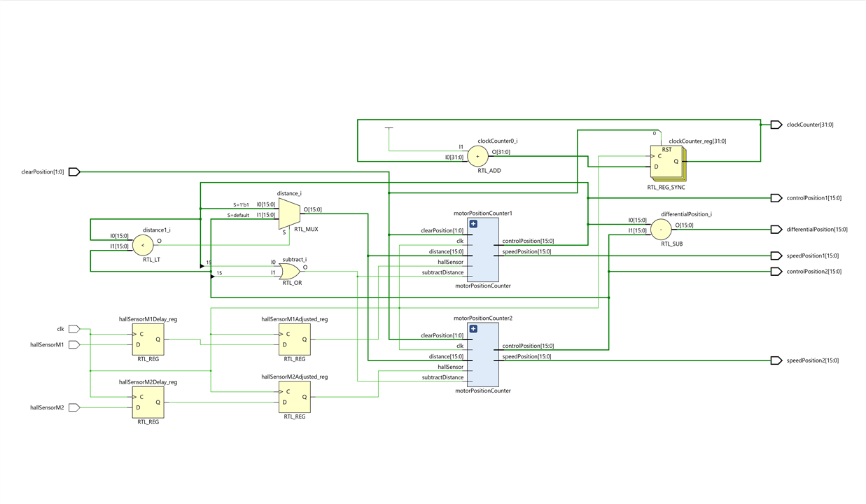
RTL Analysis and Schematic for the Differential Motors Position Module
The schematic allows us to have a more exact vision of the implementation that Vivado has made of our modules.
This is the schematic for the Differential Motors Position Module
RTL Analysis and Schematic for the Motor Position Counter Module
This is the schematic for the Motor Position Counter Module

Creation of a AXI4-Lite Interface Wrapper for the modules
We are going to create an AXI4-Lite Interface Wrapper to be able to access our top module from a bare metal application in C language built on a Microblaze softprocessor.
AXI4-Lite Interface
The AMBA AXI protocol supports high-performance, high-frequency system designs for communication between Manager and Subordinate components.
The AXI protocol:
- Permits address information to be issued ahead of the actual data transfer.
- Supports multiple outstanding transactions.
- Supports out-of-order completion of transactions
AMBA AXI4 (Advanced eXtensible Interface 4) is the fourth generation of the AMBA interface specification from ARM. AXI4-Lite is a subset of the AXI4 protocol intended for communication with simpler, smaller control register-style interfaces in components.
The key features of the AXI4-Lite interfaces are:
- All transactions are of burst length 1.
- All data accesses use the full width of the data bus: AXI4-Lite supports a data bus width of 32-bit or 64-bit.
- All accesses are Non-modifiable, Non-bufferable.
- Exclusive accesses are not supported
References: AMBA AXI and ACE Protocol Specification Version H.c (arm.com)
AXI4-Lite Interface Wrapper for Custom RTL in Vivado
With Vivado it is easy to create an Create anAXI4-Lite Interface Wrapper for Custom RTL. We are going to create a wrapper for our two Verilog modules.
Create a new AXI4 peripheral IP block for the Motor Position module.
To create a new AXI4 peripheral IP in Vivado, select Tools > Create and Package New IP...

A window will pop up in the current Vivado Project that is open with a brief summary of options available, including the option to create a new AXI4 peripheral. Click Next to continue on.
On the second page, select the option Create a new AXI4 peripheral then give the peripheral the desired name, version, and description info on the following page.

The next page allows for you to set the number of master and slave AXI interfaces the custom peripheral needs. This includes the type of AXI each interface is. In this case, only one slave AXI4-Lite interface is needed since we're just needing the C application to be able to write to a register in the RTL.
On this page, there are settings to configure such as the width of the data bus of the AXI interface and the number of registers available to write to/read from.
We will use 1 AXI Lite Slave Interface with 5 registers:
- CLEAR COUNTERS : 32 bits only two bits to reset control counters for motor1 and motor2
- M1 POSITION : 32 bits concatenation of Speed Counter (16 bits) and Control Counter (16 bits) for motor1
- M2 POSITION : 32 bits concatenation of Speed Counter (16 bits) and Control Counter (16 bits) for motor2
- POS DIFFERENCE : 32 bits concatenation of 0's (16 bits) and the difference between the two control counters
- CLOCK COUNTER : 32 bits keeps track of clock counter

Finally we add the new IP block to a local repository.

At any time we can edit our IP block by creating a temporary Vivado project from the IP catalog

For an AXI4-Lite IP project, there are two Verilog files generated:
- <peripheral_name>.v (the top level file)
<peripheral_name>_S00_AXI.v

Now we need to add our Verilog sources.
Add the input ports and instantiate our top module and wire it to the AXI Lite wrapper.
File motor_position_v1_0.v add the two user ports inputs: m1_sensor and m1_sensor
- input wire m1_sensor,
- input wire m2_sensor,
motor_position_v1_0.v
`timescale 1 ns / 1 ps

	module motor_position_v1_0 #
	(
		// Users to add parameters here

		// User parameters ends
		// Do not modify the parameters beyond this line


		// Parameters of Axi Slave Bus Interface S00_AXI
		parameter integer C_S00_AXI_DATA_WIDTH	= 32,
		parameter integer C_S00_AXI_ADDR_WIDTH	= 5
	)
	(
		// Users to add ports here
		input wire m1_sensor,
        input wire m2_sensor,

		// User ports ends
		// Do not modify the ports beyond this line


		// Ports of Axi Slave Bus Interface S00_AXI
		input wire  s00_axi_aclk,
		input wire  s00_axi_aresetn,
		input wire [C_S00_AXI_ADDR_WIDTH-1 : 0] s00_axi_awaddr,
		input wire [2 : 0] s00_axi_awprot,
		input wire  s00_axi_awvalid,
		output wire  s00_axi_awready,
		input wire [C_S00_AXI_DATA_WIDTH-1 : 0] s00_axi_wdata,
		input wire [(C_S00_AXI_DATA_WIDTH/8)-1 : 0] s00_axi_wstrb,
		input wire  s00_axi_wvalid,
		output wire  s00_axi_wready,
		output wire [1 : 0] s00_axi_bresp,
		output wire  s00_axi_bvalid,
		input wire  s00_axi_bready,
		input wire [C_S00_AXI_ADDR_WIDTH-1 : 0] s00_axi_araddr,
		input wire [2 : 0] s00_axi_arprot,
		input wire  s00_axi_arvalid,
		output wire  s00_axi_arready,
		output wire [C_S00_AXI_DATA_WIDTH-1 : 0] s00_axi_rdata,
		output wire [1 : 0] s00_axi_rresp,
		output wire  s00_axi_rvalid,
		input wire  s00_axi_rready
	);
// Instantiation of Axi Bus Interface S00_AXI
	motor_position_v1_0_S00_AXI # (
		.C_S_AXI_DATA_WIDTH(C_S00_AXI_DATA_WIDTH),
		.C_S_AXI_ADDR_WIDTH(C_S00_AXI_ADDR_WIDTH)
	) motor_position_v1_0_S00_AXI_inst (
	    .m1_sensor(m1_sensor),
        .m2_sensor(m2_sensor),
		.S_AXI_ACLK(s00_axi_aclk),
		.S_AXI_ARESETN(s00_axi_aresetn),
		.S_AXI_AWADDR(s00_axi_awaddr),
		.S_AXI_AWPROT(s00_axi_awprot),
		.S_AXI_AWVALID(s00_axi_awvalid),
		.S_AXI_AWREADY(s00_axi_awready),
		.S_AXI_WDATA(s00_axi_wdata),
		.S_AXI_WSTRB(s00_axi_wstrb),
		.S_AXI_WVALID(s00_axi_wvalid),
		.S_AXI_WREADY(s00_axi_wready),
		.S_AXI_BRESP(s00_axi_bresp),
		.S_AXI_BVALID(s00_axi_bvalid),
		.S_AXI_BREADY(s00_axi_bready),
		.S_AXI_ARADDR(s00_axi_araddr),
		.S_AXI_ARPROT(s00_axi_arprot),
		.S_AXI_ARVALID(s00_axi_arvalid),
		.S_AXI_ARREADY(s00_axi_arready),
		.S_AXI_RDATA(s00_axi_rdata),
		.S_AXI_RRESP(s00_axi_rresp),
		.S_AXI_RVALID(s00_axi_rvalid),
		.S_AXI_RREADY(s00_axi_rready)
	);

	// Add user logic here

	// User logic ends

	endmodule
Then in motor_position_v1_0_S00_AXI.v add the two user ports inputs: m1_sensor and m1_sensor
Add our logic at the end of the file.
And add the ports as parameters for the motor_position_v1_0_S00_AXI instantiation
We need to modify the motor_position_v1_0_S00_AXI file to add our logic and wire the counters to the registers.
Of the five slave registers, the first one that is read-write is left the same. For the other four we modify the definition to be able to make a concurrent assignment of the counters in the user logic section.
//-- Number of Slave Registers 5
reg [C_S_AXI_DATA_WIDTH-1:0] slv_reg0;
wire [C_S_AXI_DATA_WIDTH-1:0] slv_reg1;
wire [C_S_AXI_DATA_WIDTH-1:0] slv_reg2;
wire [C_S_AXI_DATA_WIDTH-1:0] slv_reg3;
wire [C_S_AXI_DATA_WIDTH-1:0] slv_reg4;
`timescale 1 ns / 1 ps

	module motor_position_v1_0_S00_AXI #
	(
		// Users to add parameters here

		// User parameters ends
		// Do not modify the parameters beyond this line

		// Width of S_AXI data bus
		parameter integer C_S_AXI_DATA_WIDTH	= 32,
		// Width of S_AXI address bus
		parameter integer C_S_AXI_ADDR_WIDTH	= 5
	)
	(
		// Users to add ports here
        input wire m1_sensor,
        input wire m2_sensor,

		// User ports ends
		// Do not modify the ports beyond this line

		// Global Clock Signal
		input wire  S_AXI_ACLK,
		// Global Reset Signal. This Signal is Active LOW
		input wire  S_AXI_ARESETN,
		// Write address (issued by master, acceped by Slave)
		input wire [C_S_AXI_ADDR_WIDTH-1 : 0] S_AXI_AWADDR,
		// Write channel Protection type. This signal indicates the
    		// privilege and security level of the transaction, and whether
    		// the transaction is a data access or an instruction access.
		input wire [2 : 0] S_AXI_AWPROT,
		// Write address valid. This signal indicates that the master signaling
    		// valid write address and control information.
		input wire  S_AXI_AWVALID,
		// Write address ready. This signal indicates that the slave is ready
    		// to accept an address and associated control signals.
		output wire  S_AXI_AWREADY,
		// Write data (issued by master, acceped by Slave)
		input wire [C_S_AXI_DATA_WIDTH-1 : 0] S_AXI_WDATA,
		// Write strobes. This signal indicates which byte lanes hold
    		// valid data. There is one write strobe bit for each eight
    		// bits of the write data bus.
		input wire [(C_S_AXI_DATA_WIDTH/8)-1 : 0] S_AXI_WSTRB,
		// Write valid. This signal indicates that valid write
    		// data and strobes are available.
		input wire  S_AXI_WVALID,
		// Write ready. This signal indicates that the slave
    		// can accept the write data.
		output wire  S_AXI_WREADY,
		// Write response. This signal indicates the status
    		// of the write transaction.
		output wire [1 : 0] S_AXI_BRESP,
		// Write response valid. This signal indicates that the channel
    		// is signaling a valid write response.
		output wire  S_AXI_BVALID,
		// Response ready. This signal indicates that the master
    		// can accept a write response.
		input wire  S_AXI_BREADY,
		// Read address (issued by master, acceped by Slave)
		input wire [C_S_AXI_ADDR_WIDTH-1 : 0] S_AXI_ARADDR,
		// Protection type. This signal indicates the privilege
    		// and security level of the transaction, and whether the
    		// transaction is a data access or an instruction access.
		input wire [2 : 0] S_AXI_ARPROT,
		// Read address valid. This signal indicates that the channel
    		// is signaling valid read address and control information.
		input wire  S_AXI_ARVALID,
		// Read address ready. This signal indicates that the slave is
    		// ready to accept an address and associated control signals.
		output wire  S_AXI_ARREADY,
		// Read data (issued by slave)
		output wire [C_S_AXI_DATA_WIDTH-1 : 0] S_AXI_RDATA,
		// Read response. This signal indicates the status of the
    		// read transfer.
		output wire [1 : 0] S_AXI_RRESP,
		// Read valid. This signal indicates that the channel is
    		// signaling the required read data.
		output wire  S_AXI_RVALID,
		// Read ready. This signal indicates that the master can
    		// accept the read data and response information.
		input wire  S_AXI_RREADY
	);

	// AXI4LITE signals
	reg [C_S_AXI_ADDR_WIDTH-1 : 0] 	axi_awaddr;
	reg  	axi_awready;
	reg  	axi_wready;
	reg [1 : 0] 	axi_bresp;
	reg  	axi_bvalid;
	reg [C_S_AXI_ADDR_WIDTH-1 : 0] 	axi_araddr;
	reg  	axi_arready;
	reg [C_S_AXI_DATA_WIDTH-1 : 0] 	axi_rdata;
	reg [1 : 0] 	axi_rresp;
	reg  	axi_rvalid;

	// Example-specific design signals
	// local parameter for addressing 32 bit / 64 bit C_S_AXI_DATA_WIDTH
	// ADDR_LSB is used for addressing 32/64 bit registers/memories
	// ADDR_LSB = 2 for 32 bits (n downto 2)
	// ADDR_LSB = 3 for 64 bits (n downto 3)
	localparam integer ADDR_LSB = (C_S_AXI_DATA_WIDTH/32) + 1;
	localparam integer OPT_MEM_ADDR_BITS = 2;
	//----------------------------------------------
	//-- Signals for user logic register space example
	//------------------------------------------------
	//-- Number of Slave Registers 5
	reg [C_S_AXI_DATA_WIDTH-1:0]	slv_reg0;
	wire [C_S_AXI_DATA_WIDTH-1:0]	slv_reg1;
	wire [C_S_AXI_DATA_WIDTH-1:0]	slv_reg2;
	wire [C_S_AXI_DATA_WIDTH-1:0]	slv_reg3;
	wire [C_S_AXI_DATA_WIDTH-1:0]	slv_reg4;
	wire	 slv_reg_rden;
	wire	 slv_reg_wren;
	reg [C_S_AXI_DATA_WIDTH-1:0]	 reg_data_out;
	integer	 byte_index;
	reg	 aw_en;

	// I/O Connections assignments

	assign S_AXI_AWREADY	= axi_awready;
	assign S_AXI_WREADY	= axi_wready;
	assign S_AXI_BRESP	= axi_bresp;
	assign S_AXI_BVALID	= axi_bvalid;
	assign S_AXI_ARREADY	= axi_arready;
	assign S_AXI_RDATA	= axi_rdata;
	assign S_AXI_RRESP	= axi_rresp;
	assign S_AXI_RVALID	= axi_rvalid;
	// Implement axi_awready generation
	// axi_awready is asserted for one S_AXI_ACLK clock cycle when both
	// S_AXI_AWVALID and S_AXI_WVALID are asserted. axi_awready is
	// de-asserted when reset is low.

	always @( posedge S_AXI_ACLK )
	begin
	  if ( S_AXI_ARESETN == 1'b0 )
	    begin
	      axi_awready <= 1'b0;
	      aw_en <= 1'b1;
	    end
	  else
	    begin
	      if (~axi_awready && S_AXI_AWVALID && S_AXI_WVALID && aw_en)
	        begin
	          // slave is ready to accept write address when
	          // there is a valid write address and write data
	          // on the write address and data bus. This design
	          // expects no outstanding transactions.
	          axi_awready <= 1'b1;
	          aw_en <= 1'b0;
	        end
	        else if (S_AXI_BREADY && axi_bvalid)
	            begin
	              aw_en <= 1'b1;
	              axi_awready <= 1'b0;
	            end
	      else
	        begin
	          axi_awready <= 1'b0;
	        end
	    end
	end

	// Implement axi_awaddr latching
	// This process is used to latch the address when both
	// S_AXI_AWVALID and S_AXI_WVALID are valid.

	always @( posedge S_AXI_ACLK )
	begin
	  if ( S_AXI_ARESETN == 1'b0 )
	    begin
	      axi_awaddr <= 0;
	    end
	  else
	    begin
	      if (~axi_awready && S_AXI_AWVALID && S_AXI_WVALID && aw_en)
	        begin
	          // Write Address latching
	          axi_awaddr <= S_AXI_AWADDR;
	        end
	    end
	end

	// Implement axi_wready generation
	// axi_wready is asserted for one S_AXI_ACLK clock cycle when both
	// S_AXI_AWVALID and S_AXI_WVALID are asserted. axi_wready is
	// de-asserted when reset is low.

	always @( posedge S_AXI_ACLK )
	begin
	  if ( S_AXI_ARESETN == 1'b0 )
	    begin
	      axi_wready <= 1'b0;
	    end
	  else
	    begin
	      if (~axi_wready && S_AXI_WVALID && S_AXI_AWVALID && aw_en )
	        begin
	          // slave is ready to accept write data when
	          // there is a valid write address and write data
	          // on the write address and data bus. This design
	          // expects no outstanding transactions.
	          axi_wready <= 1'b1;
	        end
	      else
	        begin
	          axi_wready <= 1'b0;
	        end
	    end
	end

	// Implement memory mapped register select and write logic generation
	// The write data is accepted and written to memory mapped registers when
	// axi_awready, S_AXI_WVALID, axi_wready and S_AXI_WVALID are asserted. Write strobes are used to
	// select byte enables of slave registers while writing.
	// These registers are cleared when reset (active low) is applied.
	// Slave register write enable is asserted when valid address and data are available
	// and the slave is ready to accept the write address and write data.
	assign slv_reg_wren = axi_wready && S_AXI_WVALID && axi_awready && S_AXI_AWVALID;

	always @( posedge S_AXI_ACLK )
	begin
	  if ( S_AXI_ARESETN == 1'b0 )
	    begin
	      slv_reg0 <= 0;
//	      slv_reg1 <= 0; /**** Assign in user logic ****/
//	      slv_reg2 <= 0; /**** Assign in user logic ****/
//	      slv_reg3 <= 0; /**** Assign in user logic ****/
//	      slv_reg4 <= 0; /**** Assign in user logic ****/
	    end
	  else begin
	    if (slv_reg_wren)
	      begin
	        case ( axi_awaddr[ADDR_LSB+OPT_MEM_ADDR_BITS:ADDR_LSB] )
	          3'h0:
	            for ( byte_index = 0; byte_index <= (C_S_AXI_DATA_WIDTH/8)-1; byte_index = byte_index+1 )
	              if ( S_AXI_WSTRB[byte_index] == 1 ) begin
	                // Respective byte enables are asserted as per write strobes
	                // Slave register 0
	                slv_reg0[(byte_index*8) +: 8] <= S_AXI_WDATA[(byte_index*8) +: 8];
	              end
	          3'h1:
	            for ( byte_index = 0; byte_index <= (C_S_AXI_DATA_WIDTH/8)-1; byte_index = byte_index+1 )
	              if ( S_AXI_WSTRB[byte_index] == 1 ) begin
	                // Respective byte enables are asserted as per write strobes
	                // Slave register 1
	                // /**** Assign in user logic ****/
	                // slv_reg1[(byte_index*8) +: 8] <= S_AXI_WDATA[(byte_index*8) +: 8];
	              end
	          3'h2:
	            for ( byte_index = 0; byte_index <= (C_S_AXI_DATA_WIDTH/8)-1; byte_index = byte_index+1 )
	              if ( S_AXI_WSTRB[byte_index] == 1 ) begin
	                // Respective byte enables are asserted as per write strobes
	                // Slave register 2
	                // /**** Assign in user logic ****/
	                // slv_reg2[(byte_index*8) +: 8] <= S_AXI_WDATA[(byte_index*8) +: 8];
	              end
	          3'h3:
	            for ( byte_index = 0; byte_index <= (C_S_AXI_DATA_WIDTH/8)-1; byte_index = byte_index+1 )
	              if ( S_AXI_WSTRB[byte_index] == 1 ) begin
	                // Respective byte enables are asserted as per write strobes
	                // Slave register 3
	                // /**** Assign in user logic ****/
	                // slv_reg3[(byte_index*8) +: 8] <= S_AXI_WDATA[(byte_index*8) +: 8];
	              end
	          3'h4:
	            for ( byte_index = 0; byte_index <= (C_S_AXI_DATA_WIDTH/8)-1; byte_index = byte_index+1 )
	              if ( S_AXI_WSTRB[byte_index] == 1 ) begin
	                // Respective byte enables are asserted as per write strobes
	                // Slave register 4
	                // /**** Assign in user logic ****/
	                // slv_reg4[(byte_index*8) +: 8] <= S_AXI_WDATA[(byte_index*8) +: 8];
	              end
	          default : begin
	                      slv_reg0 <= slv_reg0;
	                      // slv_reg1 <= slv_reg1; /**** Assign in user logic ****/
	                      // slv_reg2 <= slv_reg2; /**** Assign in user logic ****/
	                      // slv_reg3 <= slv_reg3; /**** Assign in user logic ****/
	                      // slv_reg4 <= slv_reg4; /**** Assign in user logic ****/
	                    end
	        endcase
	      end
	  end
	end

	// Implement write response logic generation
	// The write response and response valid signals are asserted by the slave
	// when axi_wready, S_AXI_WVALID, axi_wready and S_AXI_WVALID are asserted.
	// This marks the acceptance of address and indicates the status of
	// write transaction.

	always @( posedge S_AXI_ACLK )
	begin
	  if ( S_AXI_ARESETN == 1'b0 )
	    begin
	      axi_bvalid  <= 0;
	      axi_bresp   <= 2'b0;
	    end
	  else
	    begin
	      if (axi_awready && S_AXI_AWVALID && ~axi_bvalid && axi_wready && S_AXI_WVALID)
	        begin
	          // indicates a valid write response is available
	          axi_bvalid <= 1'b1;
	          axi_bresp  <= 2'b0; // 'OKAY' response
	        end                   // work error responses in future
	      else
	        begin
	          if (S_AXI_BREADY && axi_bvalid)
	            //check if bready is asserted while bvalid is high)
	            //(there is a possibility that bready is always asserted high)
	            begin
	              axi_bvalid <= 1'b0;
	            end
	        end
	    end
	end

	// Implement axi_arready generation
	// axi_arready is asserted for one S_AXI_ACLK clock cycle when
	// S_AXI_ARVALID is asserted. axi_awready is
	// de-asserted when reset (active low) is asserted.
	// The read address is also latched when S_AXI_ARVALID is
	// asserted. axi_araddr is reset to zero on reset assertion.

	always @( posedge S_AXI_ACLK )
	begin
	  if ( S_AXI_ARESETN == 1'b0 )
	    begin
	      axi_arready <= 1'b0;
	      axi_araddr  <= 32'b0;
	    end
	  else
	    begin
	      if (~axi_arready && S_AXI_ARVALID)
	        begin
	          // indicates that the slave has acceped the valid read address
	          axi_arready <= 1'b1;
	          // Read address latching
	          axi_araddr  <= S_AXI_ARADDR;
	        end
	      else
	        begin
	          axi_arready <= 1'b0;
	        end
	    end
	end

	// Implement axi_arvalid generation
	// axi_rvalid is asserted for one S_AXI_ACLK clock cycle when both
	// S_AXI_ARVALID and axi_arready are asserted. The slave registers
	// data are available on the axi_rdata bus at this instance. The
	// assertion of axi_rvalid marks the validity of read data on the
	// bus and axi_rresp indicates the status of read transaction.axi_rvalid
	// is deasserted on reset (active low). axi_rresp and axi_rdata are
	// cleared to zero on reset (active low).
	always @( posedge S_AXI_ACLK )
	begin
	  if ( S_AXI_ARESETN == 1'b0 )
	    begin
	      axi_rvalid <= 0;
	      axi_rresp  <= 0;
	    end
	  else
	    begin
	      if (axi_arready && S_AXI_ARVALID && ~axi_rvalid)
	        begin
	          // Valid read data is available at the read data bus
	          axi_rvalid <= 1'b1;
	          axi_rresp  <= 2'b0; // 'OKAY' response
	        end
	      else if (axi_rvalid && S_AXI_RREADY)
	        begin
	          // Read data is accepted by the master
	          axi_rvalid <= 1'b0;
	        end
	    end
	end

	// Implement memory mapped register select and read logic generation
	// Slave register read enable is asserted when valid address is available
	// and the slave is ready to accept the read address.
	assign slv_reg_rden = axi_arready & S_AXI_ARVALID & ~axi_rvalid;
	always @(*)
	begin
	      // Address decoding for reading registers
	      case ( axi_araddr[ADDR_LSB+OPT_MEM_ADDR_BITS:ADDR_LSB] )
	        3'h0   : reg_data_out <= slv_reg0;
	        3'h1   : reg_data_out <= slv_reg1;
	        3'h2   : reg_data_out <= slv_reg2;
	        3'h3   : reg_data_out <= slv_reg3;
	        3'h4   : reg_data_out <= slv_reg4;
	        default : reg_data_out <= 0;
	      endcase
	end

	// Output register or memory read data
	always @( posedge S_AXI_ACLK )
	begin
	  if ( S_AXI_ARESETN == 1'b0 )
	    begin
	      axi_rdata  <= 0;
	    end
	  else
	    begin
	      // When there is a valid read address (S_AXI_ARVALID) with
	      // acceptance of read address by the slave (axi_arready),
	      // output the read dada
	      if (slv_reg_rden)
	        begin
	          axi_rdata <= reg_data_out;     // register read data
	        end
	    end
	end

	// Add user logic here
   wire[1:0] clear;
   assign clear = slv_reg0[1:0];

   wire [15:0] m1_pos1, m1_pos2, m2_pos1, m2_pos2, pos_diff;
   wire [31:0] count_clk;
   assign slv_reg1 = {m1_pos1, m1_pos2};
   assign slv_reg2 = {m2_pos1, m2_pos2};
   assign slv_reg3 = {16'b0, pos_diff};
   assign slv_reg4 = count_clk;

    differentialMotorPosition differentialMotorPositionInstance (
       .clk(S_AXI_ACLK),
       .speedPosition1(m1_pos1),
       .controlPosition1(m1_pos2),
       .speedPosition2(m2_pos1),
       .controlPosition2(m2_pos2),
       .differentialPosition(pos_diff),
       .clockCounter(count_clk),
       .hallSensorM1(m1_sensor),
       .hallSensorM2(m2_sensor),
       .clearPosition(clear)
    );

	// User logic ends

	endmodule
We use the wizards proposed by the Package IP panel.

Create your Software Drivers for your IP. If you don't create them later from Vitis you can choose a generic driver by editing the BSP

Edit Software Driver
motor_position.h
#ifndef MOTOR_POSITION_H
#define MOTOR_POSITION_H


/****************** Include Files ********************/
#include "xil_types.h"
#include "xil_io.h"
#include "xstatus.h"

#define MOTOR_POSITION_S00_AXI_SLV_REG0_OFFSET 0
#define MOTOR_POSITION_S00_AXI_SLV_REG1_OFFSET 4
#define MOTOR_POSITION_S00_AXI_SLV_REG2_OFFSET 8
#define MOTOR_POSITION_S00_AXI_SLV_REG3_OFFSET 12
#define MOTOR_POSITION_S00_AXI_SLV_REG4_OFFSET 16

#define MOTOR_POSITION_CLEAR_OFFSET     MOTOR_POSITION_S00_AXI_SLV_REG0_OFFSET
#define MOTOR_POSITION_M1_POS_OFFSET    MOTOR_POSITION_S00_AXI_SLV_REG1_OFFSET
#define MOTOR_POSITION_M2_POS_OFFSET    MOTOR_POSITION_S00_AXI_SLV_REG2_OFFSET
#define MOTOR_POSITION_POS_DIFF_OFFSET  MOTOR_POSITION_S00_AXI_SLV_REG3_OFFSET
#define MOTOR_POSITION_CLK_OFFSET       MOTOR_POSITION_S00_AXI_SLV_REG4_OFFSET


typedef struct MotorPosition {
   u32 baseAddr;
   u32 clkFreqHz;
   u32 edgesPerRev;
   u32 gearboxRatio;
} MotorPosition;


/**************************** Type Definitions *****************************/
/**
 *
 * Write a value to a MOTOR_POSITION register. A 32 bit write is performed.
 * If the component is implemented in a smaller width, only the least
 * significant data is written.
 *
 * @param   BaseAddress is the base address of the MOTOR_POSITIONdevice.
 * @param   RegOffset is the register offset from the base to write to.
 * @param   Data is the data written to the register.
 *
 * @return  None.
 *
 * @note
 * C-style signature:
 * 	void MOTOR_POSITION_mWriteReg(u32 BaseAddress, unsigned RegOffset, u32 Data)
 *
 */
#define MOTOR_POSITION_mWriteReg(BaseAddress, RegOffset, Data) \
  	Xil_Out32((BaseAddress) + (RegOffset), (u32)(Data))

/**
 *
 * Read a value from a MOTOR_POSITION register. A 32 bit read is performed.
 * If the component is implemented in a smaller width, only the least
 * significant data is read from the register. The most significant data
 * will be read as 0.
 *
 * @param   BaseAddress is the base address of the MOTOR_POSITION device.
 * @param   RegOffset is the register offset from the base to write to.
 *
 * @return  Data is the data from the register.
 *
 * @note
 * C-style signature:
 * 	u32 MOTOR_POSITION_mReadReg(u32 BaseAddress, unsigned RegOffset)
 *
 */
#define MOTOR_POSITION_mReadReg(BaseAddress, RegOffset) \
    Xil_In32((BaseAddress) + (RegOffset))

/************************** Function Prototypes ****************************/
/**
 *
 * Run a self-test on the driver/device. Note this may be a destructive test if
 * resets of the device are performed.
 *
 * If the hardware system is not built correctly, this function may never
 * return to the caller.
 *
 * @param   baseaddr_p is the base address of the MOTOR_POSITION instance to be worked on.
 *
 * @return
 *
 *    - XST_SUCCESS   if all self-test code passed
 *    - XST_FAILURE   if any self-test code failed
 *
 * @note    Caching must be turned off for this function to work.
 * @note    Self test may fail if data memory and device are not on the same bus.
 *
 */
XStatus MOTOR_POSITION_Reg_SelfTest(void * baseaddr_p);

void MOTOR_POSITION_init(MotorPosition* motorPosition, u32 baseAddr,
      u32 clkFreqHz, u32 edgesPerRev, u32 gearboxRatio);

void MOTOR_POSITION_getSpeeds(MotorPosition* motorPosition, int motor_speed[]);

int16_t MOTOR_POSITION_getDistanceTraveled(MotorPosition* motorPosition);

void MOTOR_POSITION_getEdgeCounts(MotorPosition* motorPosition, int m1[],
      int m2[]);

void MOTOR_POSITION_clearSpeedCounters(MotorPosition* motorPosition) ;

void MOTOR_POSITION_getPositions(MotorPosition* motorPosition,
      int16_t motor_pos[]);

int16_t MOTOR_POSITION_getPositionDifference(MotorPosition* motorPosition);

void MOTOR_POSITION_clearPosCounter(MotorPosition* motorPosition);

#endif // MOTOR_POSITION_H
motor_position.c
/***************************** Include Files *******************************/
#include "motor_position.h"

/************************** Function Definitions ***************************/

void MOTOR_POSITION_init(MotorPosition* motorPosition, u32 baseAddr,
      u32 clkFreqHz, u32 edgesPerRev, u32 gearboxRatio) {
   motorPosition->baseAddr = baseAddr;
   motorPosition->clkFreqHz = clkFreqHz;
   motorPosition->edgesPerRev = edgesPerRev;
   motorPosition->gearboxRatio = gearboxRatio;
}

void MOTOR_POSITION_getSpeeds(MotorPosition* motorPosition, int motor_speed[]) {
   int m1[2];
   int m2[2];
   MOTOR_POSITION_getEdgeCounts(motorPosition, m1, m2);
   double conversionFactor = 60.0 * motorPosition->clkFreqHz
                                  / motorPosition->edgesPerRev
                                  / motorPosition->gearboxRatio;
   motor_speed[0] = conversionFactor * m1[0] / m1[1];
   motor_speed[1] = conversionFactor * m2[0] / m2[1];
   MOTOR_POSITION_clearSpeedCounters(motorPosition);
}

int16_t MOTOR_POSITION_getDistanceTraveled(MotorPosition* motorPosition) {
   int16_t motor_pos[2];
   MOTOR_POSITION_getPositions(motorPosition, motor_pos);
   return (motor_pos[0] + motor_pos[1]) / 2;
}

void MOTOR_POSITION_getEdgeCounts(MotorPosition* motorPosition, int m1[],
      int m2[]) {
   u32 m1Pos_addr = motorPosition->baseAddr + MOTOR_POSITION_M1_POS_OFFSET;
   u32 m2Pos_addr = motorPosition->baseAddr + MOTOR_POSITION_M2_POS_OFFSET;
   u32 clk_addr   = motorPosition->baseAddr + MOTOR_POSITION_CLK_OFFSET;
   m1[0] = (int) (Xil_In32(m1Pos_addr) >> 16);
   m1[1] = (int)  Xil_In32(clk_addr);
   m2[0] = (int) (Xil_In32(m2Pos_addr) >> 16);
   m2[1] = (int)  Xil_In32(clk_addr);
}

void MOTOR_POSITION_clearSpeedCounters(MotorPosition* motorPosition) {
   Xil_Out8(motorPosition->baseAddr + MOTOR_POSITION_CLEAR_OFFSET, 0x1);
   Xil_Out8(motorPosition->baseAddr + MOTOR_POSITION_CLEAR_OFFSET, 0x0);
}

void MOTOR_POSITION_getPositions(MotorPosition* motorPosition,
      int16_t motor_pos[]) {
   u32 m1Pos_addr = motorPosition->baseAddr + MOTOR_POSITION_M1_POS_OFFSET;
   u32 m2Pos_addr = motorPosition->baseAddr + MOTOR_POSITION_M2_POS_OFFSET;
   motor_pos[0] = Xil_In16(m1Pos_addr);
   motor_pos[1] = Xil_In16(m2Pos_addr);
}

int16_t MOTOR_POSITION_getPositionDifference(MotorPosition* motorPosition) {
   u32 pos_diff_addr = motorPosition->baseAddr + MOTOR_POSITION_POS_DIFF_OFFSET;
   return (int16_t) Xil_In16(pos_diff_addr);
}

void MOTOR_POSITION_clearPosCounter(MotorPosition* motorPosition) {
   Xil_Out8(motorPosition->baseAddr + MOTOR_POSITION_CLEAR_OFFSET, 0x2);
   Xil_Out8(motorPosition->baseAddr + MOTOR_POSITION_CLEAR_OFFSET, 0x0);
}
Create a self test procedure motor_position_selftest.c
/***************************** Include Files *******************************/
#include "motor_position.h"
#include "xparameters.h"
#include "stdio.h"
#include "xil_io.h"

/************************** Constant Definitions ***************************/
#define READ_WRITE_MUL_FACTOR 0x10

/************************** Function Definitions ***************************/
/**
 *
 * Run a self-test on the driver/device. Note this may be a destructive test if
 * resets of the device are performed.
 *
 * If the hardware system is not built correctly, this function may never
 * return to the caller.
 *
 * @param   baseaddr_p is the base address of the MOTOR_POSITIONinstance to be worked on.
 *
 * @return
 *
 *    - XST_SUCCESS   if all self-test code passed
 *    - XST_FAILURE   if any self-test code failed
 *
 * @note    Caching must be turned off for this function to work.
 * @note    Self test may fail if data memory and device are not on the same bus.
 *
 */
XStatus MOTOR_POSITION_Reg_SelfTest(void * baseaddr_p)
{
	u32 baseaddr;
	int write_loop_index;
	int read_loop_index;
	int Index;

	baseaddr = (u32) baseaddr_p;

	xil_printf("******************************\n\r");
	xil_printf("* User Peripheral Self Test\n\r");
	xil_printf("******************************\n\n\r");

	/*
	 * Write to user logic slave module register(s) and read back
	 */
	xil_printf("User logic slave module test...\n\r");

	for (write_loop_index = 0 ; write_loop_index < 1; write_loop_index++)
	  MOTOR_POSITION_mWriteReg (baseaddr, write_loop_index*4, (write_loop_index+1)*READ_WRITE_MUL_FACTOR);
	for (read_loop_index = 0 ; read_loop_index < 1; read_loop_index++)
	  if ( MOTOR_POSITION_mReadReg (baseaddr, read_loop_index*4) != (read_loop_index+1)*READ_WRITE_MUL_FACTOR){
	    xil_printf ("Error reading register value at address %x\n", (int)baseaddr + read_loop_index*4);
	    return XST_FAILURE;
	  }

	xil_printf("   - slave register write/read passed\n\n\r");

	return XST_SUCCESS;
}
Review and Package IP

You can now add this IP repository to any Vivado project.

Add the new IP to design. Search motor_position

Run Connection Automation and made external the other two inputs, m1_sensor and m2_sensor

New board connections
We will connect the motor sensors to the Arty S7's shield connector.
The Arty S7's shield connector is implemented on headers J1, J2, J3, J5, J6, and J8.

We will add two new connections from the shield connector to the Motor Drive and Power Distribution Board
| MDPDB | Arty S7 | PACKAGE PIN |
| PWM Right | IO0 | L13 |
| DIR Right | IO1 | N13 |
| nSLEEP Right | IO2 | L16 |
| PWM Left | IO3 | R14 |
| DIR Left | IO4 | T14 |
| nSLEEP Left | IO5 | R16 |
| ERA Right | IO6 | R17 |
| ELA Left | IO7 | V17 |
Add new constrains for the to external ports m1_sensor_0 and m2_sensor_0
set_property -dict { PACKAGE_PIN R17   IOSTANDARD LVCMOS33 } [get_ports { m1_sensor_0 }]; #IO_L14N_T2_SRCC_14      Sch=ck_io[6]
set_property -dict { PACKAGE_PIN V17   IOSTANDARD LVCMOS33 } [get_ports { m2_sensor_0 }]; #IO_L16N_T2_A15_D31_14   Sch=ck_io[7]
New constrain file
## This file is a general .xdc for the Arty S7-50 Rev. E
## To use it in a project:
## - uncomment the lines corresponding to used pins
## - rename the used ports (in each line, after get_ports) according to the top level signal names in the project

## Clock Signals
#set_property -dict { PACKAGE_PIN F14   IOSTANDARD LVCMOS33 } [get_ports { CLK12MHZ }]; #IO_L13P_T2_MRCC_15 Sch=uclk
#create_clock -add -name sys_clk_pin -period 83.333 -waveform {0 41.667} [get_ports { CLK12MHZ }];
#set_property -dict { PACKAGE_PIN R2    IOSTANDARD SSTL135 } [get_ports { CLK100MHZ }]; #IO_L12P_T1_MRCC_34 Sch=ddr3_clk[200]
#create_clock -add -name sys_clk_pin -period 10.000 -waveform {0 5.000}  [get_ports { CLK100MHZ }];

## Switches
#set_property -dict { PACKAGE_PIN H14   IOSTANDARD LVCMOS33 } [get_ports { sw[0] }]; #IO_L20N_T3_A19_15 Sch=sw[0]
#set_property -dict { PACKAGE_PIN H18   IOSTANDARD LVCMOS33 } [get_ports { sw[1] }]; #IO_L21P_T3_DQS_15 Sch=sw[1]
#set_property -dict { PACKAGE_PIN G18   IOSTANDARD LVCMOS33 } [get_ports { sw[2] }]; #IO_L21N_T3_DQS_A18_15 Sch=sw[2]
#set_property -dict { PACKAGE_PIN M5    IOSTANDARD SSTL135 } [get_ports { sw[3] }]; #IO_L6N_T0_VREF_34 Sch=sw[3]

## RGB LEDs
#set_property -dict { PACKAGE_PIN J15   IOSTANDARD LVCMOS33 } [get_ports { led0_r }]; #IO_L23N_T3_FWE_B_15 Sch=led0_r
#set_property -dict { PACKAGE_PIN G17   IOSTANDARD LVCMOS33 } [get_ports { led0_g }]; #IO_L14N_T2_SRCC_15 Sch=led0_g
#set_property -dict { PACKAGE_PIN F15   IOSTANDARD LVCMOS33 } [get_ports { led0_b }]; #IO_L13N_T2_MRCC_15 Sch=led0_b
#set_property -dict { PACKAGE_PIN E15   IOSTANDARD LVCMOS33 } [get_ports { led1_r }]; #IO_L15N_T2_DQS_ADV_B_15 Sch=led1_r
#set_property -dict { PACKAGE_PIN F18   IOSTANDARD LVCMOS33 } [get_ports { led1_g }]; #IO_L16P_T2_A28_15 Sch=led1_g
#set_property -dict { PACKAGE_PIN E14   IOSTANDARD LVCMOS33 } [get_ports { led1_b }]; #IO_L15P_T2_DQS_15 Sch=led1_b

## LEDs
#set_property -dict { PACKAGE_PIN E18   IOSTANDARD LVCMOS33 } [get_ports { led[0] }]; #IO_L16N_T2_A27_15 Sch=led[2]
#set_property -dict { PACKAGE_PIN F13   IOSTANDARD LVCMOS33 } [get_ports { led[1] }]; #IO_L17P_T2_A26_15 Sch=led[3]
#set_property -dict { PACKAGE_PIN E13   IOSTANDARD LVCMOS33 } [get_ports { led[2] }]; #IO_L17N_T2_A25_15 Sch=led[4]
#set_property -dict { PACKAGE_PIN H15   IOSTANDARD LVCMOS33 } [get_ports { led[3] }]; #IO_L18P_T2_A24_15 Sch=led[5]

## Buttons
#set_property -dict { PACKAGE_PIN G15   IOSTANDARD LVCMOS33 } [get_ports { btn[0] }]; #IO_L18N_T2_A23_15 Sch=btn[0]
#set_property -dict { PACKAGE_PIN K16   IOSTANDARD LVCMOS33 } [get_ports { btn[1] }]; #IO_L19P_T3_A22_15 Sch=btn[1]
#set_property -dict { PACKAGE_PIN J16   IOSTANDARD LVCMOS33 } [get_ports { btn[2] }]; #IO_L19N_T3_A21_VREF_15 Sch=btn[2]
#set_property -dict { PACKAGE_PIN H13   IOSTANDARD LVCMOS33 } [get_ports { btn[3] }]; #IO_L20P_T3_A20_15 Sch=btn[3]

## Pmod Header JA
#set_property -dict { PACKAGE_PIN L17   IOSTANDARD LVCMOS33 } [get_ports { ja[0] }]; #IO_L4P_T0_D04_14 Sch=ja_p[1]
#set_property -dict { PACKAGE_PIN L18   IOSTANDARD LVCMOS33 } [get_ports { ja[1] }]; #IO_L4N_T0_D05_14 Sch=ja_n[1]
#set_property -dict { PACKAGE_PIN M14   IOSTANDARD LVCMOS33 } [get_ports { ja[2] }]; #IO_L5P_T0_D06_14 Sch=ja_p[2]
#set_property -dict { PACKAGE_PIN N14   IOSTANDARD LVCMOS33 } [get_ports { ja[3] }]; #IO_L5N_T0_D07_14 Sch=ja_n[2]
#set_property -dict { PACKAGE_PIN M16   IOSTANDARD LVCMOS33 } [get_ports { ja[4] }]; #IO_L7P_T1_D09_14 Sch=ja_p[3]
#set_property -dict { PACKAGE_PIN M17   IOSTANDARD LVCMOS33 } [get_ports { ja[5] }]; #IO_L7N_T1_D10_14 Sch=ja_n[3]
#set_property -dict { PACKAGE_PIN M18   IOSTANDARD LVCMOS33 } [get_ports { ja[6] }]; #IO_L8P_T1_D11_14 Sch=ja_p[4]
#set_property -dict { PACKAGE_PIN N18   IOSTANDARD LVCMOS33 } [get_ports { ja[7] }]; #IO_L8N_T1_D12_14 Sch=ja_n[4]

## Pmod Header JB
#set_property -dict { PACKAGE_PIN P17   IOSTANDARD LVCMOS33 } [get_ports { jb[0] }]; #IO_L9P_T1_DQS_14 Sch=jb_p[1]
#set_property -dict { PACKAGE_PIN P18   IOSTANDARD LVCMOS33 } [get_ports { jb[1] }]; #IO_L9N_T1_DQS_D13_14 Sch=jb_n[1]
#set_property -dict { PACKAGE_PIN R18   IOSTANDARD LVCMOS33 } [get_ports { jb[2] }]; #IO_L10P_T1_D14_14 Sch=jb_p[2]
#set_property -dict { PACKAGE_PIN T18   IOSTANDARD LVCMOS33 } [get_ports { jb[3] }]; #IO_L10N_T1_D15_14 Sch=jb_n[2]
#set_property -dict { PACKAGE_PIN P14   IOSTANDARD LVCMOS33 } [get_ports { jb[4] }]; #IO_L11P_T1_SRCC_14 Sch=jb_p[3]
#set_property -dict { PACKAGE_PIN P15   IOSTANDARD LVCMOS33 } [get_ports { jb[5] }]; #IO_L11N_T1_SRCC_14 Sch=jb_n[3]
#set_property -dict { PACKAGE_PIN N15   IOSTANDARD LVCMOS33 } [get_ports { jb[6] }]; #IO_L12P_T1_MRCC_14 Sch=jb_p[4]
#set_property -dict { PACKAGE_PIN P16   IOSTANDARD LVCMOS33 } [get_ports { jb[7] }]; #IO_L12N_T1_MRCC_14 Sch=jb_n[4]

## Pmod Header JC
#set_property -dict { PACKAGE_PIN U15   IOSTANDARD LVCMOS33 } [get_ports { jc[0] }]; #IO_L18P_T2_A12_D28_14 Sch=jc1/ck_io[41]
#set_property -dict { PACKAGE_PIN V16   IOSTANDARD LVCMOS33 } [get_ports { jc[1] }]; #IO_L18N_T2_A11_D27_14 Sch=jc2/ck_io[40]
#set_property -dict { PACKAGE_PIN U17   IOSTANDARD LVCMOS33 } [get_ports { jc[2] }]; #IO_L15P_T2_DQS_RDWR_B_14 Sch=jc3/ck_io[39]
#set_property -dict { PACKAGE_PIN U18   IOSTANDARD LVCMOS33 } [get_ports { jc[3] }]; #IO_L15N_T2_DQS_DOUT_CSO_B_14 Sch=jc4/ck_io[38]
#set_property -dict { PACKAGE_PIN U16   IOSTANDARD LVCMOS33 } [get_ports { jc[4] }]; #IO_L16P_T2_CSI_B_14 Sch=jc7/ck_io[37]
#set_property -dict { PACKAGE_PIN P13   IOSTANDARD LVCMOS33 } [get_ports { jc[5] }]; #IO_L19P_T3_A10_D26_14 Sch=jc8/ck_io[36]
#set_property -dict { PACKAGE_PIN R13   IOSTANDARD LVCMOS33 } [get_ports { jc[6] }]; #IO_L19N_T3_A09_D25_VREF_14 Sch=jc9/ck_io[35]
#set_property -dict { PACKAGE_PIN V14   IOSTANDARD LVCMOS33 } [get_ports { jc[7] }]; #IO_L20P_T3_A08_D24_14 Sch=jc10/ck_io[34]

## Pmod Header JD
#set_property -dict { PACKAGE_PIN V15   IOSTANDARD LVCMOS33 } [get_ports { jd[0] }]; #IO_L20N_T3_A07_D23_14 Sch=jd1/ck_io[33]
#set_property -dict { PACKAGE_PIN U12   IOSTANDARD LVCMOS33 } [get_ports { jd[1] }]; #IO_L21P_T3_DQS_14 Sch=jd2/ck_io[32]
#set_property -dict { PACKAGE_PIN V13   IOSTANDARD LVCMOS33 } [get_ports { jd[2] }]; #IO_L21N_T3_DQS_A06_D22_14 Sch=jd3/ck_io[31]
#set_property -dict { PACKAGE_PIN T12   IOSTANDARD LVCMOS33 } [get_ports { jd[3] }]; #IO_L22P_T3_A05_D21_14 Sch=jd4/ck_io[30]
#set_property -dict { PACKAGE_PIN T13   IOSTANDARD LVCMOS33 } [get_ports { jd[4] }]; #IO_L22N_T3_A04_D20_14 Sch=jd7/ck_io[29]
#set_property -dict { PACKAGE_PIN R11   IOSTANDARD LVCMOS33 } [get_ports { jd[5] }]; #IO_L23P_T3_A03_D19_14 Sch=jd8/ck_io[28]
#set_property -dict { PACKAGE_PIN T11   IOSTANDARD LVCMOS33 } [get_ports { jd[6] }]; #IO_L23N_T3_A02_D18_14 Sch=jd9/ck_io[27]
#set_property -dict { PACKAGE_PIN U11   IOSTANDARD LVCMOS33 } [get_ports { jd[7] }]; #IO_L24P_T3_A01_D17_14 Sch=jd10/ck_io[26]

## USB-UART Interface
#set_property -dict { PACKAGE_PIN R12   IOSTANDARD LVCMOS33 } [get_ports { uart_rxd_out }]; #IO_25_14 Sch=uart_rxd_out
#set_property -dict { PACKAGE_PIN V12   IOSTANDARD LVCMOS33 } [get_ports { uart_txd_in }]; #IO_L24N_T3_A00_D16_14 Sch=uart_txd_in

## ChipKit Outer Digital Header
# Right Motor Control
set_property -dict { PACKAGE_PIN L13   IOSTANDARD LVCMOS33 } [get_ports { pwm0_0 }]; #IO_0_14 Sch=ck_io[0]
set_property -dict { PACKAGE_PIN N13   IOSTANDARD LVCMOS33 } [get_ports { hbridge_control_tri_o[0] }]; #IO_L6N_T0_D08_VREF_14   Sch=ck_io[1]
set_property -dict { PACKAGE_PIN L16   IOSTANDARD LVCMOS33 } [get_ports { hbridge_control_tri_o[1] }]; #IO_L3N_T0_DQS_EMCCLK_14 Sch=ck_io[2]
# Left motor Control
set_property -dict { PACKAGE_PIN R14   IOSTANDARD LVCMOS33 } [get_ports { pwm0_1 }]; #IO_L13P_T2_MRCC_14      Sch=ck_io[3]
set_property -dict { PACKAGE_PIN T14   IOSTANDARD LVCMOS33 } [get_ports { hbridge_control_tri_o[2] }]; #IO_L13N_T2_MRCC_14      Sch=ck_io[4]
set_property -dict { PACKAGE_PIN R16   IOSTANDARD LVCMOS33 } [get_ports { hbridge_control_tri_o[3] }]; #IO_L14P_T2_SRCC_14      Sch=ck_io[5]

set_property -dict { PACKAGE_PIN R17   IOSTANDARD LVCMOS33 } [get_ports { m1_sensor_0 }]; #IO_L14N_T2_SRCC_14      Sch=ck_io[6]
set_property -dict { PACKAGE_PIN V17   IOSTANDARD LVCMOS33 } [get_ports { m2_sensor_0 }]; #IO_L16N_T2_A15_D31_14   Sch=ck_io[7]
#set_property -dict { PACKAGE_PIN R15   IOSTANDARD LVCMOS33 } [get_ports { ck_io8 }]; #IO_L17P_T2_A14_D30_14   Sch=ck_io[8]
#set_property -dict { PACKAGE_PIN T15   IOSTANDARD LVCMOS33 } [get_ports { ck_io9 }]; #IO_L17N_T2_A13_D29_14   Sch=ck_io[9]

## ChipKit SPI Header
## NOTE: The ChipKit SPI header ports can also be used as digital I/O and share FPGA pins with ck_io10-13. Do not use both at the same time.
#set_property -dict { PACKAGE_PIN H16   IOSTANDARD LVCMOS33 } [get_ports { ck_io10_ss   }]; #IO_L22P_T3_A17_15   Sch=ck_io10_ss
#set_property -dict { PACKAGE_PIN H17   IOSTANDARD LVCMOS33 } [get_ports { ck_io11_mosi }]; #IO_L22N_T3_A16_15   Sch=ck_io11_mosi
#set_property -dict { PACKAGE_PIN K14   IOSTANDARD LVCMOS33 } [get_ports { ck_io12_miso }]; #IO_L23P_T3_FOE_B_15 Sch=ck_io12_miso
#set_property -dict { PACKAGE_PIN G16   IOSTANDARD LVCMOS33 } [get_ports { ck_io13_sck  }]; #IO_L14P_T2_SRCC_15  Sch=ck_io13_sck

## ChipKit Inner Digital Header
## Note: these pins are shared with PMOD Headers JC and JD and cannot be used at the same time as the applicable PMOD interface(s)
#set_property -dict { PACKAGE_PIN U11   IOSTANDARD LVCMOS33 } [get_ports { ck_io26 }]; #IO_L24P_T3_A01_D17_14        Sch=jd10/ck_io[26]
#set_property -dict { PACKAGE_PIN T11   IOSTANDARD LVCMOS33 } [get_ports { ck_io27 }]; #IO_L23N_T3_A02_D18_14        Sch=jd9/ck_io[27]
#set_property -dict { PACKAGE_PIN R11   IOSTANDARD LVCMOS33 } [get_ports { ck_io28 }]; #IO_L23P_T3_A03_D19_14        Sch=jd8/ck_io[28]
#set_property -dict { PACKAGE_PIN T13   IOSTANDARD LVCMOS33 } [get_ports { ck_io29 }]; #IO_L22N_T3_A04_D20_14        Sch=jd7/ck_io[29]
#set_property -dict { PACKAGE_PIN T12   IOSTANDARD LVCMOS33 } [get_ports { ck_io30 }]; #IO_L22P_T3_A05_D21_14        Sch=jd4/ck_io[30]
#set_property -dict { PACKAGE_PIN V13   IOSTANDARD LVCMOS33 } [get_ports { ck_io31 }]; #IO_L21N_T3_DQS_A06_D22_14    Sch=jd3/ck_io[31]
#set_property -dict { PACKAGE_PIN U12   IOSTANDARD LVCMOS33 } [get_ports { ck_io32 }]; #IO_L21P_T3_DQS_14            Sch=jd2/ck_io[32]
#set_property -dict { PACKAGE_PIN V15   IOSTANDARD LVCMOS33 } [get_ports { ck_io33 }]; #IO_L20N_T3_A07_D23_14        Sch=jd1/ck_io[33]
#set_property -dict { PACKAGE_PIN V14   IOSTANDARD LVCMOS33 } [get_ports { ck_io34 }]; #IO_L20P_T3_A08_D24_14        Sch=jc10/ck_io[34]
#set_property -dict { PACKAGE_PIN R13   IOSTANDARD LVCMOS33 } [get_ports { ck_io35 }]; #IO_L19N_T3_A09_D25_VREF_14   Sch=jc9/ck_io[35]
#set_property -dict { PACKAGE_PIN P13   IOSTANDARD LVCMOS33 } [get_ports { ck_io36 }]; #IO_L19P_T3_A10_D26_14        Sch=jc8/ck_io[36]
#set_property -dict { PACKAGE_PIN U16   IOSTANDARD LVCMOS33 } [get_ports { ck_io37 }]; #IO_L16P_T2_CSI_B_14          Sch=jc7/ck_io[37]
#set_property -dict { PACKAGE_PIN U18   IOSTANDARD LVCMOS33 } [get_ports { ck_io38 }]; #IO_L15N_T2_DQS_DOUT_CSO_B_14 Sch=jc4/ck_io[38]
#set_property -dict { PACKAGE_PIN U17   IOSTANDARD LVCMOS33 } [get_ports { ck_io39 }]; #IO_L15P_T2_DQS_RDWR_B_14     Sch=jc3/ck_io[39]
#set_property -dict { PACKAGE_PIN V16   IOSTANDARD LVCMOS33 } [get_ports { ck_io40 }]; #IO_L18N_T2_A11_D27_14        Sch=jc2/ck_io[40]
#set_property -dict { PACKAGE_PIN U15   IOSTANDARD LVCMOS33 } [get_ports { ck_io41 }]; #IO_L18P_T2_A12_D28_14        Sch=jc1/ck_io[41]

## Dedicated Analog Inputs
#set_property -dict { PACKAGE_PIN J10   } [get_ports { vp_in }]; #IO_L1P_T0_AD4P_35 Sch=v_p
#set_property -dict { PACKAGE_PIN K9    } [get_ports { vn_in }]; #IO_L1N_T0_AD4N_35 Sch=v_n

## ChipKit Outer Analog Header - as Single-Ended Analog Inputs
## NOTE: These ports can be used as single-ended analog inputs with voltages from 0-3.3V (ChipKit analog pins A0-A5) or as digital I/O.
## WARNING: Do not use both sets of constraints at the same time!
## NOTE: The following constraints should be used with the XADC IP core when using these ports as analog inputs.
#set_property -dict { PACKAGE_PIN B13   IOSTANDARD LVCMOS33 } [get_ports { vaux0_p  }]; #IO_L1P_T0_AD0P_15     Sch=ck_an_p[0]   ChipKit pin=A0
#set_property -dict { PACKAGE_PIN A13   IOSTANDARD LVCMOS33 } [get_ports { vaux0_n  }]; #IO_L1N_T0_AD0N_15     Sch=ck_an_n[0]   ChipKit pin=A0
#set_property -dict { PACKAGE_PIN B15   IOSTANDARD LVCMOS33 } [get_ports { vaux1_p  }]; #IO_L3P_T0_DQS_AD1P_15 Sch=ck_an_p[1]   ChipKit pin=A1
#set_property -dict { PACKAGE_PIN A15   IOSTANDARD LVCMOS33 } [get_ports { vaux1_n  }]; #IO_L3N_T0_DQS_AD1N_15 Sch=ck_an_n[1]   ChipKit pin=A1
#set_property -dict { PACKAGE_PIN E12   IOSTANDARD LVCMOS33 } [get_ports { vaux9_p  }]; #IO_L5P_T0_AD9P_15     Sch=ck_an_p[2]   ChipKit pin=A2
#set_property -dict { PACKAGE_PIN D12   IOSTANDARD LVCMOS33 } [get_ports { vaux9_n  }]; #IO_L5N_T0_AD9N_15     Sch=ck_an_n[2]   ChipKit pin=A2
#set_property -dict { PACKAGE_PIN B17   IOSTANDARD LVCMOS33 } [get_ports { vaux2_p  }]; #IO_L7P_T1_AD2P_15     Sch=ck_an_p[3]   ChipKit pin=A3
#set_property -dict { PACKAGE_PIN A17   IOSTANDARD LVCMOS33 } [get_ports { vaux2_n  }]; #IO_L7N_T1_AD2N_15     Sch=ck_an_n[3]   ChipKit pin=A3
#set_property -dict { PACKAGE_PIN C17   IOSTANDARD LVCMOS33 } [get_ports { vaux10_p }]; #IO_L8P_T1_AD10P_15    Sch=ck_an_p[4]   ChipKit pin=A4
#set_property -dict { PACKAGE_PIN B18   IOSTANDARD LVCMOS33 } [get_ports { vaux10_n }]; #IO_L8N_T1_AD10N_15    Sch=ck_an_n[4]   ChipKit pin=A4
#set_property -dict { PACKAGE_PIN E16   IOSTANDARD LVCMOS33 } [get_ports { vaux11_p }]; #IO_L10P_T1_AD11P_15   Sch=ck_an_p[5]   ChipKit pin=A5
#set_property -dict { PACKAGE_PIN E17   IOSTANDARD LVCMOS33 } [get_ports { vaux11_n }]; #IO_L10N_T1_AD11N_15   Sch=ck_an_n[5]   ChipKit pin=A5
## ChipKit Outer Analog Header - as Digital I/O
## NOTE: The following constraints should be used when using these ports as digital I/O.
#set_property -dict { PACKAGE_PIN G13   IOSTANDARD LVCMOS33 } [get_ports { ck_a0 }]; #IO_0_15            Sch=ck_a[0]
#set_property -dict { PACKAGE_PIN B16   IOSTANDARD LVCMOS33 } [get_ports { ck_a1 }]; #IO_L4P_T0_15       Sch=ck_a[1]
#set_property -dict { PACKAGE_PIN A16   IOSTANDARD LVCMOS33 } [get_ports { ck_a2 }]; #IO_L4N_T0_15       Sch=ck_a[2]
#set_property -dict { PACKAGE_PIN C13   IOSTANDARD LVCMOS33 } [get_ports { ck_a3 }]; #IO_L6P_T0_15       Sch=ck_a[3]
#set_property -dict { PACKAGE_PIN C14   IOSTANDARD LVCMOS33 } [get_ports { ck_a4 }]; #IO_L6N_T0_VREF_15  Sch=ck_a[4]
#set_property -dict { PACKAGE_PIN D18   IOSTANDARD LVCMOS33 } [get_ports { ck_a5 }]; #IO_L11P_T1_SRCC_15 Sch=ck_a[5]

## ChipKit Inner Analog Header - as Differential Analog Inputs
## NOTE: These ports can be used as differential analog inputs with voltages from 0-1.0V (ChipKit analog pins A6-A11) or as digital I/O.
## WARNING: Do not use both sets of constraints at the same time!
## NOTE: The following constraints should be used with the XADC core when using these ports as analog inputs.
#set_property -dict { PACKAGE_PIN B14   IOSTANDARD LVCMOS33 } [get_ports { vaux8_p }]; #IO_L2P_T0_AD8P_15     Sch=ad_p[8]   ChipKit pin=A6
#set_property -dict { PACKAGE_PIN A14   IOSTANDARD LVCMOS33 } [get_ports { vaux8_n }]; #IO_L2N_T0_AD8N_15     Sch=ad_n[8]   ChipKit pin=A7
#set_property -dict { PACKAGE_PIN D16   IOSTANDARD LVCMOS33 } [get_ports { vaux3_p }]; #IO_L9P_T1_DQS_AD3P_15 Sch=ad_p[3]   ChipKit pin=A8
#set_property -dict { PACKAGE_PIN D17   IOSTANDARD LVCMOS33 } [get_ports { vaux3_n }]; #IO_L9N_T1_DQS_AD3N_15 Sch=ad_n[3]   ChipKit pin=A9
## ChipKit Inner Analog Header - as Digital I/O
## NOTE: The following constraints should be used when using the inner analog header ports as digital I/O.
#set_property -dict { PACKAGE_PIN B14   IOSTANDARD LVCMOS33 } [get_ports { ck_a6  }]; #IO_L2P_T0_AD8P_15     Sch=ad_p[8]
#set_property -dict { PACKAGE_PIN A14   IOSTANDARD LVCMOS33 } [get_ports { ck_a7  }]; #IO_L2N_T0_AD8N_15     Sch=ad_n[8]
#set_property -dict { PACKAGE_PIN D16   IOSTANDARD LVCMOS33 } [get_ports { ck_a8  }]; #IO_L9P_T1_DQS_AD3P_15 Sch=ad_p[3]
#set_property -dict { PACKAGE_PIN D17   IOSTANDARD LVCMOS33 } [get_ports { ck_a9  }]; #IO_L9N_T1_DQS_AD3N_15 Sch=ad_n[3]
#set_property -dict { PACKAGE_PIN D14   IOSTANDARD LVCMOS33 } [get_ports { ck_a10 }]; #IO_L12P_T1_MRCC_15    Sch=ck_a10_r   (Cannot be used as an analog input)
#set_property -dict { PACKAGE_PIN D15   IOSTANDARD LVCMOS33 } [get_ports { ck_a11 }]; #IO_L12N_T1_MRCC_15    Sch=ck_a11_r   (Cannot be used as an analog input)

## ChipKit I2C
#set_property -dict { PACKAGE_PIN J14   IOSTANDARD LVCMOS33 } [get_ports { ck_scl }]; #IO_L24N_T3_RS0_15 Sch=ck_scl
#set_property -dict { PACKAGE_PIN J13   IOSTANDARD LVCMOS33 } [get_ports { ck_sda }]; #IO_L24P_T3_RS1_15 Sch=ck_sda

## Misc. ChipKit Ports
#set_property -dict { PACKAGE_PIN K13   IOSTANDARD LVCMOS33 } [get_ports { ck_ioa }]; #IO_25_15 Sch=ck_ioa
#set_property -dict { PACKAGE_PIN C18   IOSTANDARD LVCMOS33 } [get_ports { ck_rst }]; #IO_L11N_T1_SRCC_15

## Quad SPI Flash
## Note: the SCK clock signal can be driven using the STARTUPE2 primitive
#set_property -dict { PACKAGE_PIN M13   IOSTANDARD LVCMOS33 } [get_ports { qspi_cs }]; #IO_L6P_T0_FCS_B_14 Sch=qspi_cs
#set_property -dict { PACKAGE_PIN K17   IOSTANDARD LVCMOS33 } [get_ports { qspi_dq[0] }]; #IO_L1P_T0_D00_MOSI_14 Sch=qspi_dq[0]
#set_property -dict { PACKAGE_PIN K18   IOSTANDARD LVCMOS33 } [get_ports { qspi_dq[1] }]; #IO_L1N_T0_D01_DIN_14 Sch=qspi_dq[1]
#set_property -dict { PACKAGE_PIN L14   IOSTANDARD LVCMOS33 } [get_ports { qspi_dq[2] }]; #IO_L2P_T0_D02_14 Sch=qspi_dq[2]
#set_property -dict { PACKAGE_PIN M15   IOSTANDARD LVCMOS33 } [get_ports { qspi_dq[3] }]; #IO_L2N_T0_D03_14 Sch=qspi_dq[3]

## Configuration options, can be used for all designs
set_property BITSTREAM.CONFIG.CONFIGRATE 50 [current_design]
set_property CONFIG_VOLTAGE 3.3 [current_design]
set_property CFGBVS VCCO [current_design]
set_property BITSTREAM.CONFIG.SPI_BUSWIDTH 4 [current_design]
set_property CONFIG_MODE SPIx4 [current_design]

## SW3 is assigned to a pin M5 in the 1.35v bank. This pin can also be used as
## the VREF for BANK 34. To ensure that SW3 does not define the reference voltage
## and to be able to use this pin as an ordinary I/O the following property must
## be set to enable an internal VREF for BANK 34. Since a 1.35v supply is being
## used the internal reference is set to half that value (i.e. 0.675v). Note that
## this property must be set even if SW3 is not used in the design.
set_property INTERNAL_VREF 0.675 [get_iobanks 34]
Finally Generate Bitstream and Export Hardware including the bitstream
Vitis Application C Code
We can now got to Vitis and create a new Application Project or update the last one used for testing the pwm signals.
First identify Base Address for the MOTOR_POSITION in the xparameters.h
/* Definitions for peripheral MOTOR_POSITION_0 */
#define XPAR_MOTOR_POSITION_0_S00_AXI_BASEADDR 0x44A00000
#define XPAR_MOTOR_POSITION_0_S00_AXI_HIGHADDR 0x44A0FFFF
Base Address is 0x44A00000
We have defined five registers at offsets 0x0, 0x4, 0x8, and 0x1C and 0x10.
Register offsets for Motor Position AXI GPIO registers. Look motor_positiojn.h file header
#define MOTOR_POSITION_S00_AXI_SLV_REG0_OFFSET 0
#define MOTOR_POSITION_S00_AXI_SLV_REG1_OFFSET 4
#define MOTOR_POSITION_S00_AXI_SLV_REG2_OFFSET 8
#define MOTOR_POSITION_S00_AXI_SLV_REG3_OFFSET 12
#define MOTOR_POSITION_S00_AXI_SLV_REG4_OFFSET 16
| AXI GPIO REGISTER | OFFSET | HEADER FILE |
| CLEAR COUNTERS | 0X00 | MOTOR_POSITION_S00_AXI_SLV_REG0_OFFSET |
| MOTOR1 POSITION | 0x04 | MOTOR_POSITION_S00_AXI_SLV_REG1_OFFSET |
| MOTOR2 POSITION | 0x08 | MOTOR_POSITION_S00_AXI_SLV_REG2_OFFSET |
| POSITION DIFFERENCE | 0x0C | MOTOR_POSITION_S00_AXI_SLV_REG3_OFFSET |
| CLOCK COUNTER | 0x10 | MOTOR_POSITION_S00_AXI_SLV_REG4_OFFSET |
status = MOTOR_POSITION_Reg_SelfTest(XPAR_MOTOR_POSITION_0_S00_AXI_BASEADDR);

And finally we use the Waveform Generator from the Analog Discovery 2 to stimulate the two motor sensor inputs.

Our module works. Ready to measure rotational speeds and relative position of the two wheels.

/*
 * ------------------------------------------------
 * | UART TYPE   BAUD RATE                        |
 * ------------------------------------------------
 *   uartns550   9600
 *   uartlite    Configurable only in HW design
 *   ps7_uart    115200 (configured by bootrom/bsp)
 */

#include <stdio.h>
#include "platform.h"
#include "xil_printf.h"
#include "sleep.h"
#include "xtmrctr.h"
#include "xgpio.h"
#include "xil_types.h"
#include "motor_position.h"

#define RIGHTMOTORTMRCTR_DEVICE_ID        XPAR_TMRCTR_0_DEVICE_ID
#define LEFTMOTORTMRCTR_DEVICE_ID         XPAR_TMRCTR_1_DEVICE_ID
#define PWM_PERIOD              10000000     /* PWM period in (10 ms) */
#define TMRCTR_0                0            /* Timer 0 ID */
#define TMRCTR_1                1            /* Timer 1 ID */
#define CYCLE_PER_DUTYCYCLE     10           /* Clock cycles per duty cycle */
#define MAX_DUTYCYCLE           100          /* Max duty cycle */
#define DUTYCYCLE_DIVISOR       MAX_DUTYCYCLE/* Duty cycle Divisor */

#define PERCENTAGE_INCREMENTS   10

#define BTN_MASK 0b1111
#define LED_MASK 0b1111
#define BTN1_MASK 0b0001
#define BTN2_MASK 0b0010
#define BTN3_MASK 0b0100
#define BTN4_MASK 0b1000
#define LED1_MASK 0b0001
#define LED2_MASK 0b0010
#define LED3_MASK 0b0100
#define LED4_MASK 0b1000

// Get device IDs from xparameters.h
#define BTN_ID XPAR_AXI_GPIO_0_DEVICE_ID
#define LED_ID XPAR_AXI_GPIO_1_DEVICE_ID
#define BTN_CHANNEL 1
#define LED_CHANNEL 2


#define MOTORPOSITION_BASEADDR    XPAR_MOTOR_POSITION_0_S00_AXI_BASEADDR

// Register offsets for MotorPosition's AXI GPIO registers
#define MOTORPOSITION_EDGES_PER_REVOLUTION 3
#define MOTORPOSITION_GEAR_BOX_RATIO       120

XGpio_Config *cfg_ptr;
XGpio led_device, btn_device;

XTmrCtr RightMotorTimer;
XTmrCtr LeftMotorTimer;

void setPwm_DutyCyclePercentage(XTmrCtr* MotorTimer,
		u8 percentage) {
	u32 period;
	u32 highTime;
	if (percentage >= DUTYCYCLE_DIVISOR) {
		percentage = 99;
	} else if (percentage < 0) {
		percentage = 0;
	}
	/* Disable PWM for reconfiguration if percentage == 0 disable pwm */
	XTmrCtr_PwmDisable(&*MotorTimer);
	/* Configure PWM */
	if (percentage > 0) {
		period = PWM_PERIOD;
		highTime = (period / DUTYCYCLE_DIVISOR) * percentage ;
		XTmrCtr_PwmConfigure(&*MotorTimer, period, highTime);
		/* Enable PWM after reconfiguration */
		XTmrCtr_PwmEnable(&*MotorTimer);
	}
}

int main() {
	u8 percentageRightMotor;
	u8 percentageLeftMotor;
	int status;

	u64 timeCounterMillis;
	u32 buttonsState;

	int button1State;
	int lastbutton1State = 0;

	int button2State;
	int lastbutton2State = 0;

	int button3State;
	int lastbutton3State = 0;

	int button4State;
	int lastbutton4State = 0;
	int m1[2];
	int m2[2];

	init_platform();


	print("Initializing LED Device...\r\n");

	// Initialize LED Device
	cfg_ptr = XGpio_LookupConfig(LED_ID);
	XGpio_CfgInitialize(&led_device, cfg_ptr, cfg_ptr->BaseAddress);

	print("Initializing the Button Device\r\n");

	// Initialize Button Device
	cfg_ptr = XGpio_LookupConfig(BTN_ID);
	XGpio_CfgInitialize(&btn_device, cfg_ptr, cfg_ptr->BaseAddress);

	// Set Button Tristate
	XGpio_SetDataDirection(&btn_device, BTN_CHANNEL, BTN_MASK);

	// Set Led Tristate
	XGpio_SetDataDirection(&led_device, LED_CHANNEL, 0);

	print("Initializing the Timer Counter...\r\n");
	/*
	 * Initialize the timer counter so that it's ready to use,
	 * specify the device ID that is generated in xparameters.h
	 */
	status = XTmrCtr_Initialize(&RightMotorTimer, RIGHTMOTORTMRCTR_DEVICE_ID);


	if (status != XST_SUCCESS) {
		return XST_FAILURE;
	}

	status = XTmrCtr_Initialize(&LeftMotorTimer, LEFTMOTORTMRCTR_DEVICE_ID);


	if (status != XST_SUCCESS) {
		return XST_FAILURE;
	}

	print("Timer Counter initialized\r\n");
	percentageRightMotor = 0;
	percentageLeftMotor = 0;


	setPwm_DutyCyclePercentage(&RightMotorTimer, percentageRightMotor);
	setPwm_DutyCyclePercentage(&LeftMotorTimer, percentageLeftMotor);

	status = MOTOR_POSITION_Reg_SelfTest(XPAR_MOTOR_POSITION_0_S00_AXI_BASEADDR);

	MotorPosition motorPosition;
	MOTOR_POSITION_init(&motorPosition, XPAR_MOTOR_POSITION_0_S00_AXI_BASEADDR,
			XPAR_CPU_CORE_CLOCK_FREQ_HZ, MOTORPOSITION_EDGES_PER_REVOLUTION, MOTORPOSITION_GEAR_BOX_RATIO);

	while (1) {

		// read buttons
		buttonsState = XGpio_DiscreteRead(&btn_device, BTN_CHANNEL);

//		//if button 4 is pressed exit
//		if (buttonsState & BTN4_MASK) {
//			print("exiting\r\n");
//			// exit
//			break;
//		}

		// check button 0 for incrementing duty dycle percentage for Right motor
		button1State = buttonsState & BTN1_MASK;
		//if button 1 low to high edge
		if ((button1State != lastbutton1State) && button1State && timeCounterMillis > 100) {
		//if (buttonsState & BTN1_MASK && timeCounterMillis > 100) {
			print("Increment Right Motor duty cycle units\r\n");
			timeCounterMillis = 0;
			if ( percentageRightMotor < 100) {
				percentageRightMotor = percentageRightMotor + PERCENTAGE_INCREMENTS;
				setPwm_DutyCyclePercentage(&RightMotorTimer, percentageRightMotor);
			}
			MOTOR_POSITION_getEdgeCounts(&motorPosition, m1, m2);
			xil_printf ("Get Edge Counts M1 = %d / %d M2 = %d / %d\r\n", m1[0], m1[1], m2[0], m2[1]);
			int16_t difference = MOTOR_POSITION_getPositionDifference(&motorPosition);
			xil_printf ("Difference = %d \r\n",difference);

			MOTOR_POSITION_clearSpeedCounters(&motorPosition);
			MOTOR_POSITION_clearPosCounter(&motorPosition);
			MOTOR_POSITION_getEdgeCounts(&motorPosition, m1,
					m2);
			xil_printf ("Clear M1 = %d / %d M2 = %d / %d\r\n", m1[0], m1[1], m2[0], m2[1]);


		}
		lastbutton1State = button1State;

		// check button 1 for decrementing duty dycle percentage for Right motor
		button2State = buttonsState & BTN2_MASK;
		//if button 1 low to high edge
		if ((button2State != lastbutton2State) && button2State && timeCounterMillis > 100) {
		//if (buttonsState & BTN2_MASK && timeCounterMillis > 100) {
			print("Decrement Right Motor duty cycle units\r\n");
			timeCounterMillis = 0;
			if ( percentageRightMotor > 0) {
				percentageRightMotor = percentageRightMotor - PERCENTAGE_INCREMENTS;
				setPwm_DutyCyclePercentage(&RightMotorTimer, percentageRightMotor);
			}
		}
		lastbutton3State = button3State;

		// check button 3 for incrementing duty dycle percentage for Left motor
		button3State = buttonsState & BTN3_MASK;
		//if button 3 low to high edge
		if ((button3State != lastbutton3State) && button3State && timeCounterMillis > 100) {
		//if (buttonsState & BTN1_MASK && timeCounterMillis > 100) {
			print("Increment Left Motor duty cycle units\r\n");
			timeCounterMillis = 0;
			if ( percentageLeftMotor < 100) {
				percentageLeftMotor = percentageLeftMotor + PERCENTAGE_INCREMENTS;
				setPwm_DutyCyclePercentage(&LeftMotorTimer, percentageLeftMotor);
			}
		}
		lastbutton3State = button3State;

		// check button 4 for decrementing duty dycle percentage for Left motor
		button4State = buttonsState & BTN4_MASK;
		//if button 1 low to high edge
		if ((button4State != lastbutton4State) && button4State && timeCounterMillis > 100) {
		//if (buttonsState & BTN2_MASK && timeCounterMillis > 100) {
			print("Decrement Left Motor duty cycle units\r\n");
			timeCounterMillis = 0;
			if ( percentageLeftMotor > 0) {
				percentageLeftMotor = percentageLeftMotor - PERCENTAGE_INCREMENTS;
				setPwm_DutyCyclePercentage(&LeftMotorTimer, percentageLeftMotor);
			}
		}
		lastbutton4State = button4State;


		usleep(1000);
		++timeCounterMillis;

	}

	cleanup_platform();
	return 0;
}
Conclusion
It's been quite a long post since the creation of the modules in Verilog, their testing and simulation. The construction of the wrapper for the AXI4 Lite IP Peripheral interface. The elaboration of a software driver in C and the verification of the module in the Arty S7 board.
We already have several modules made in hardware that work in parallel and outside the Microblaze softprocessor. Two dedicated to generating the PWM signal that controls the speed of the motor and another one that receives the stimuli from the sensors added to the motors and that will allow us to carry out a PID control system for the speed of the motors and to control the position of the wheels.
The next step will be to develop the library for the Artybot movement control system.
References
- AXI4-Lite Interface Wrapper for Custom RTL in Vivado 2021.2 - Hackster.io
- Using Test Benches and Stimulus Files (xilinx.com)
- Writing Efficient Test Benches
- Pololu - Romi Encoder Pair Kit, 12 CPR, 3.5-18V
- Pololu - 120:1 Mini Plastic Gearmotor HP
- Offset 3mm D-Shaft Output, Extended Motor Shaft
- Pololu Wheel 70×8mm Pair - White
- Pmod DHB1 Reference Manual - Digilent Reference
- Digilent, a National Instruments Company