


Introduction
In the previous two blog posts, we first started with creating a basic hardware platform for the Ultra96v2
Path to Programmable III: Ultra96v2 Basic Hardware Platform - Vivado 2022.2
This was followed by creating our first application running on the A53 processor
Path to Programmable III: Ultra96v2 Starter Application A53 cores - Vitis 2022.2
This application was running on a single core of the A53 application processor. The ZU3EG FPGA inside the Ultra96v2 contains a total of 4 x A53 cores (application processors) and 2 x R5 cores (Real Time processors). Clearly we were using only one out of the 6 hard processors inside the FPGA.
In this blog post I want to explore running applications on two cores at the same time with some type of memory sharing between them for communication. I will be using one R5 core and one A53 core. The ultimate aim would be to, for example, run a real time control algorithm on the R5 core, while running some vision or higher level control application on the A53 core(s). In this post we will create a much more basic application to learn how to accomplish running codes in parallel on two cores with some simple communication between the two.
Btw, what we are trying to do is referred to as AMP (Asymmetric Multi Processing) and there are much more detailed documentation made available by AMD on this. AMD provides an OpenAMP library to support complex cases of AMP, however, for this post we will go for the simplest possible way.
Lastly, a word of caution before we proceed. I am not an expert at this (not even close). So there might be mistakes in my methodology. I am just going to share what I have learnt. So take the information in this blog post with a "grain of salt" and if you spot errors, please do leave a comment about it (thanks!).
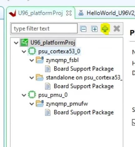
Adding a domain for R5 core
We continue here where we left off in the previous post. We had already created a basic "baremetal" application running on a single A53 core. We want to run the second application on one of the R5 cores. To do this, we need to create a separate domain for the R5 core we're going to use.
Inside VITIS, in the platform project explorer window, click the green "+" (Add Domain) button to add a new domain.
Then we fill in an appropriate name and select "psu_cortexr5_0" (First out of the two cortex r5 cores) as our target processor core. Then press Ok to create this domain.
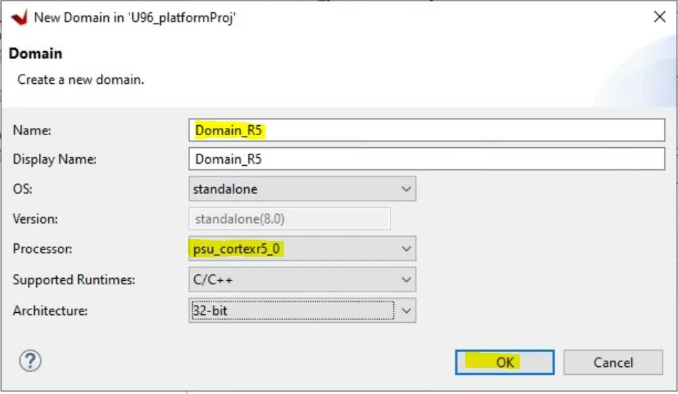
VITIS will take a few seconds to create and add this domain, and now we can see it under the platform.
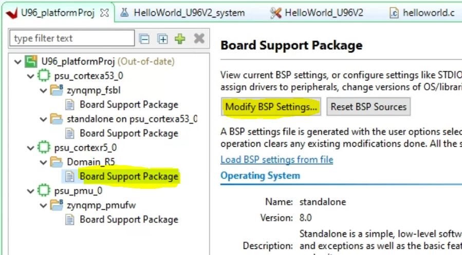
For this new platform also, let's set UART1 as the stdin and stdout. Select the "Board Support Package" under the psu_cortexr5_0 processor and click "Modify BSP settings"
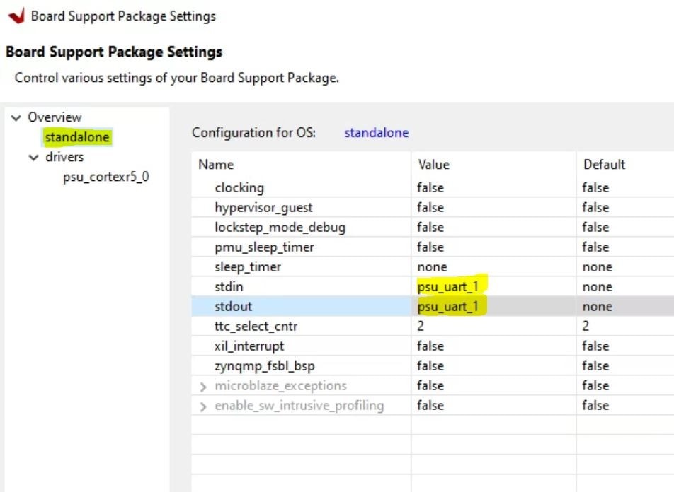
Now we can fix the stdin and stdout settings as in image below. Then press OK to close.
Create new application for R5
Now that we have a new domain created, we can create a new application that uses this newly created domain.
This will follow the same process as we used to create an application for the A53, with the only difference being that we will target the new R5 core's domain.

Nothing to do on the first page
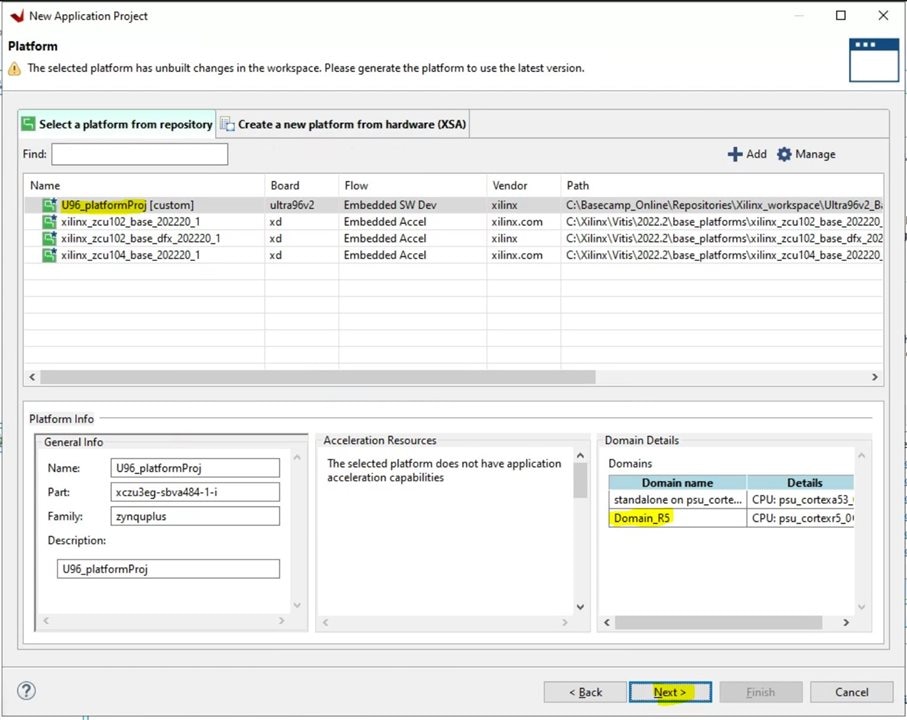
We select the same platform project that we create earlier. This time, we can see the R5 domain under "Domain details". Press Next to continue.
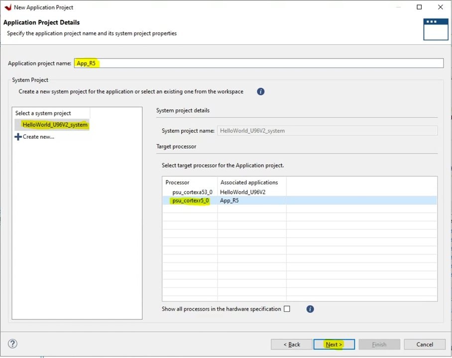
Give an appropriate name to our app that is going to run on the R5.
Select the previously created system project, and click the psu_cortexr5_0 as the target processor. The new app's name will appear in front. We also see the name of our previously created app for A53 in front of the psu_cortexa53_0 processor. Click Next to proceed.
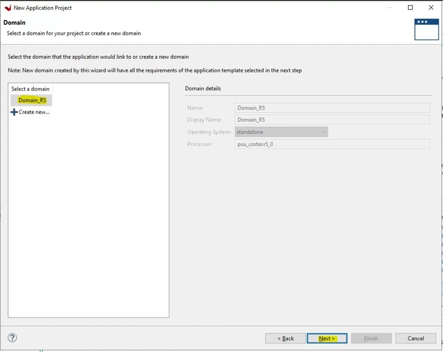
VITIS automatically selects the correct domain for this. Press Next.
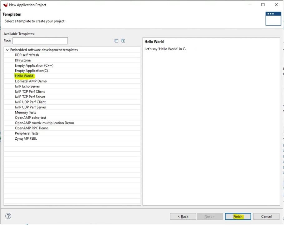
Select the Hello World template and click Finish.
This finishes the process of creating an app for the R5 processor.
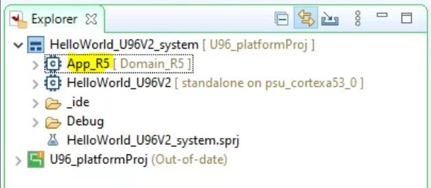
We can see this new app in our "system" along with the previously created A53 app.
The projects are showing out-of-date. We can right-click and click build so that they get up to date. This will take a few minutes to complete. Once done, the "out-of-date" text will disappear.
Running the two applications simultaneously
Before we run the applications simultaneously, we need to make sure they are not running on the same addresses in memory, as that will cause a conflict. For this, we need to look at the linker scripts.
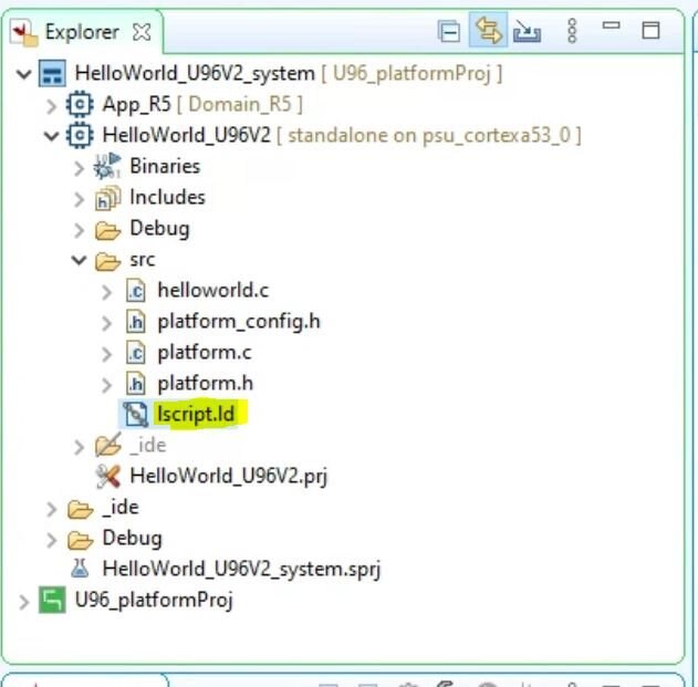
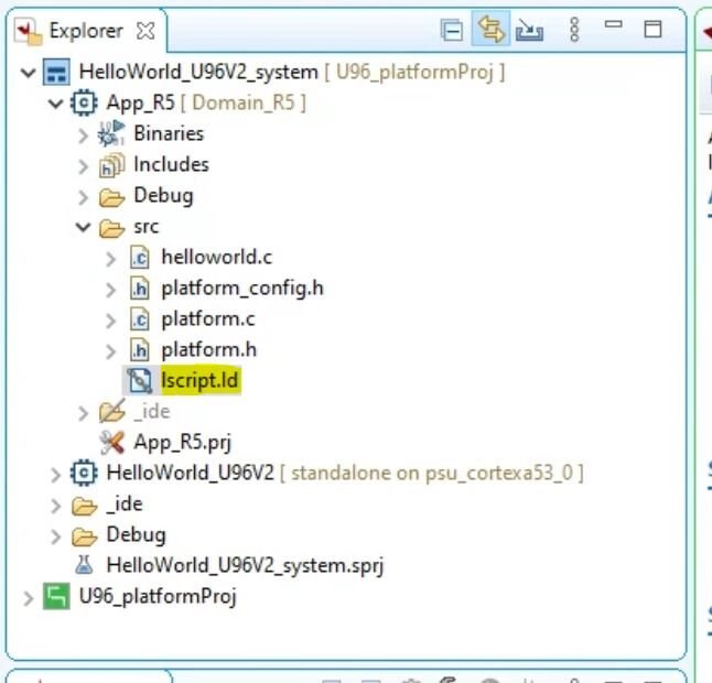
First we see the linker script for the A53 application. Double click "lscript.ld" under the A53 application to open the linker script editor.
This opens the linker script editor in VITIS.
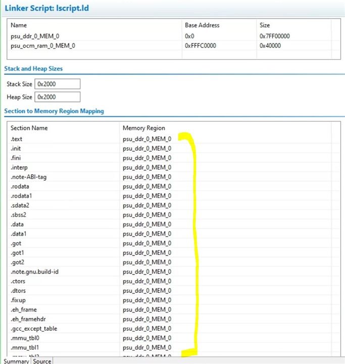
The main thing to see here is that everything on the A53 is using the psu_DDR memory. There is also an on chip memory that is available but not being uses (psu_ocm_ram_0_MEM_0)
Next we open the linker script for the R5 core application
Now we can see the memory allocations for the R5 application
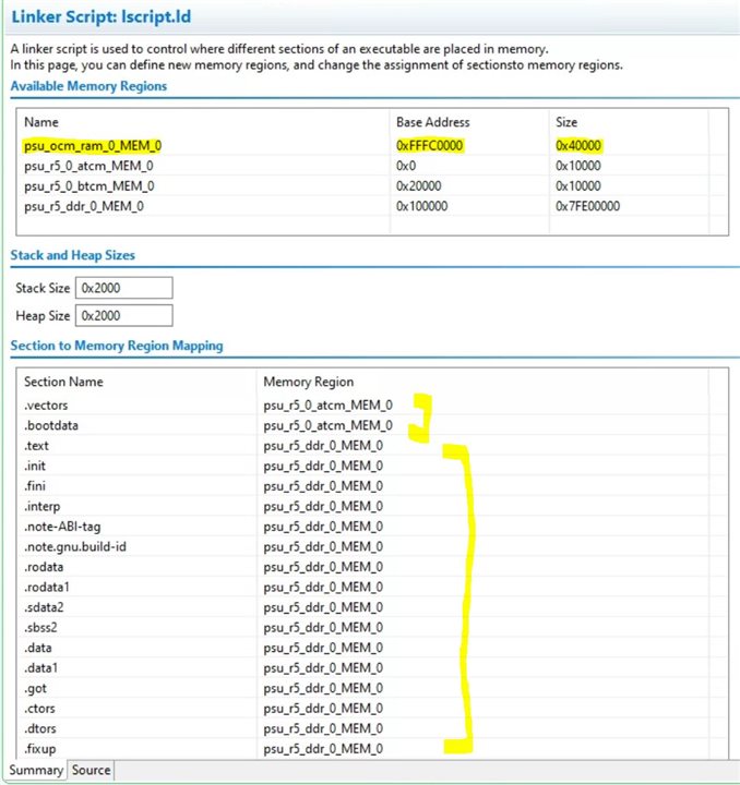
The main thing to see is that most of the sections here are also using the DDR memory, however the start addresses are different and there is enough gap between them for our simple application that the program will not overlap. ATCM is low latency memory dedicated to the R5. Note that a more proper way would be to assign completely different address ranges on the DDR to the two processors.
Also note that the R5 also has access to the same OCM memory as the A53. The start and size of this is the same in both linker scripts. Note the :Base Address for psu_ocm_ram_0_MEM_0 as we will use this later to share memory between the two cores.
With nothing to be changed for the linker scripts, those can be closed now.
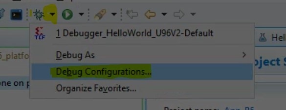
To launch the two applications, we can modify the build configuration we created previously when we launched the A53 application.
Click the drop down arrow next to the Debug icon and click "Debug configurations"
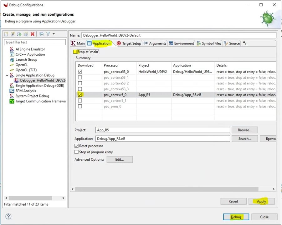
This opens up the Debug Configurations window.
Select the Application tab and
- Un-select "Stop at main" to make it easier to see result later without having to resume each core manually.
- Click the Download checkbox next to psu_cortexr5_0. Once you do this, the name of the R5 application we created will be automatically populated.
- Click Apply, and then click Debug
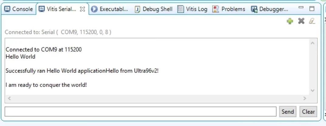
At this point, you should have the board powered up and connected via USB-JTAG just like we did in the previous blog post before launching the application. Also make sure the Vitis Serial terminal is connected to the UART com port.
VITIS will load the FPGA configuration and both applications, and execute them both.
In the serial console, we should see two hello world messages. You may recognize one of them as the custom message we wrote in the A53 application in the previous blog post. The other one is the default Hello world message from the application running on the R5.
Core-core communication
Until now, we have manged to run both applications together, but there is no communication between them. We can't simply create a global variable in C and share it across the cores, since their scope is limited to each core that its running on.
For communicating between the cores, we will use the OCM (on chip memory) that both the cores can see. We will simply create a variable in both the A53 as well as the R5 programs. This variable in both cases will be pointing to the same address the OCM. This variable will get updated by one of the applications (let's say the A53 application) and the other application will read, print and modify it, and this process will continue happening in loops running on both the processor cores.
The modified Hello world code for the A53 application is as following:
#include <stdio.h>
#include "platform.h"
#include "xil_printf.h"
#include "xil_mmu.h"
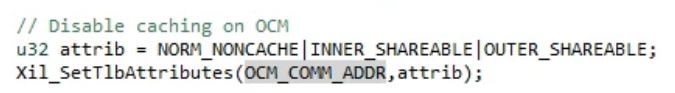
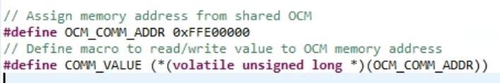
// Assign memory address from shared OCM
#define OCM_COMM_ADDR 0xFFE00000
// Define macro to read/write value to OCM memory address
#define COMM_VALUE (*(volatile unsigned long *)(OCM_COMM_ADDR))
int main()
{
init_platform();
print("Hello World from A53\n\r");
// Disable caching on OCM
u32 attrib = NORM_NONCACHE|INNER_SHAREABLE|OUTER_SHAREABLE;
Xil_SetTlbAttributes(OCM_COMM_ADDR,attrib);
for (int a = 0; a<10; a++)
{
xil_printf("%d\n",COMM_VALUE);
COMM_VALUE+=9;
sleep(1);
}
print("\n\rA53 is done\n\r ");
cleanup_platform();
return 0;
}
The modified hello world for the R5 application is as following:
#include <stdio.h>
#include "platform.h"
#include "xil_printf.h"


// Assign memory address from shared OCM
#define OCM_COMM_ADDR 0xFFE00000
// Define macro to read/write value to OCM memory address
#define COMM_VALUE (*(volatile unsigned long *)(OCM_COMM_ADDR))

int main()
{
    init_platform();

    print("Hello World from R5\n\r");

    COMM_VALUE = 0;

    for (int a = 0; a<10; a++)
    {
    	COMM_VALUE++;
    	sleep(1);
    }

    print("\n\rR5 is done \n\r");
    cleanup_platform();
    return 0;
}
I have added comments to the code to explain what is going on. The important parts are as following:
First we choose a memory location from the range allocated to the OCM in the linker script. Then we use a macro to read/write values to that memory location. Note that BOTH the R5 and A53 applications MUST use the same memory addresses for these shared variables.
The other very important lines of code are the following:

These lines are disabling the cache on the OCM share memory location we chose. I got the exact lines from some AMD forum posts (although I could have worked it out from the relevant documents). One important point to note: All memory settings are for 2MB blocks, thus to modify OCM (0xFFFC0000 to FFFFFFFF) the mmu settings should start at 0xFFE00000.
Once the code files are modified, we need to build both the applications again (Right click -> Build)
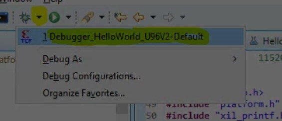
Now we can launch the previously created debug configuration again to launch the applications on both cores
It takes VITIS a minute to launch again. Once launched, we see the following in the Vitis Serial Terminal:
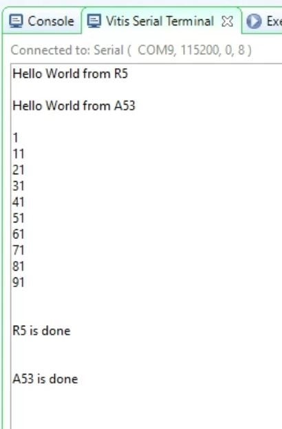
As expected, we get 10 numbers printed because the loops in both applications are running 10 times.
In each iteration, the A53 application increases the value of shared variable by 1 and goes to sleep for a second.
The R5 application, in each iteration, reads this shared variable value and prints it. It then adds 9 to it. Thus we see an increase of 10 every time (+1 by A53, +9 by R5).
This proves that our shared memory based messaging is working as expected, and both our processors are executing the applications simultaneously. In a real life project, we can assign flags to bits in the shared memory for passing control flags between the processes, and variables pointing to the shared memory to pass parameter values. This can be a simple but powerful way to maximize usage of all the available cores!
Thank you for reading and following along!