Table of Contents
Introduction
Moving on with the exploration of FPGAs, I stumbled upon this question of what really can FPGAs can do and where they fit in - unlike many of the projects built using them which can also be done on a fairly mid-range microcontroller these days. A quick search on this topic shows some of the high-speed communication protocols, usage of SerDes, multi-gigabit ethernet and optical links, extremely capable digital signal processing and floating point operations etc.
Reading through the hardware, and software tutorials and learning about vivado-vitis codesign, usage of IP blocks for PWM, serial protocols and I/O interfaces have been insightful and two of my previous blog are on these. This one will spin a little offside looking into the full-fledged capabilities of the Zynq-7000 SoC. This blog will be heavily dependent on ug585-Zynq-7000-TRM references.
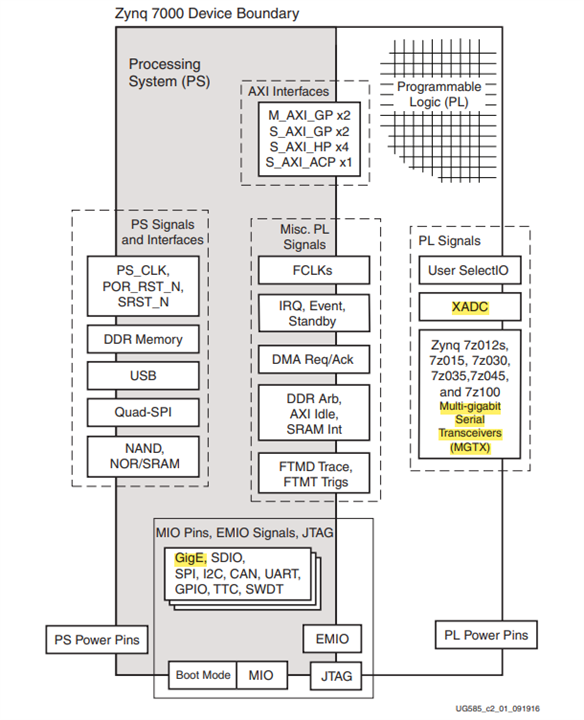
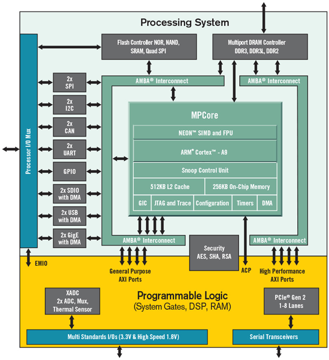
This block diagram shows signals, pins and interfaces in the Zynq 7000 and highlighted are some exotic features for which these SoCs are preferred. We'll look at 1G and higher ethernet interface, gigabit serial transceivers(JESD, PCIe implementations) and Neon engine linking to the ARM core in PS section.
1G Ethernet
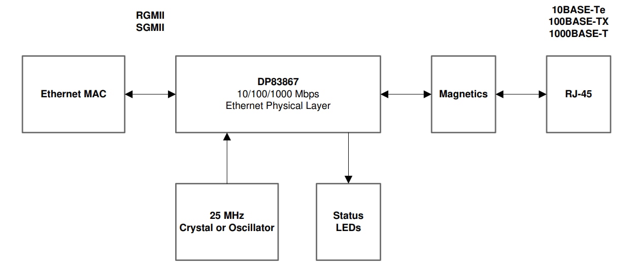
Gigabit ethernet is a common system block used when it comes to a system requiring a speedy network link. There are two Gigabit Ethernet Controllers(GEM0, GEM1) in the Zynq SoC’s Processor System. Each of these controllers can be configured and used independently. The Gigabit Ethernet Controller implements a MAC(Media Access Controller) which forms part of the data link layer in the 7-layer OSI model. For the Physical layer, an external chip like DP83867E is to be used which links the external RJ-45 ethernet port to the MAC layer in the SoC via multiplexed I/O(MIO) through interfaces like Reduced Gigabit Media Independent Interface(RGMII).

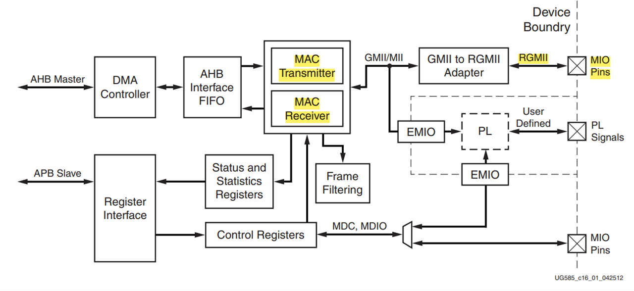
The below image shows the overall 1G ethernet application using a TI DP83867 PHY chip. The Ethernet MAC block on the left is within the Zynq 7000 SoC and further upper OSI layers are implemented thereby.
Interestingly, the further range of Zynq devices like Ultrascale+ comes with 10G/SFP capabilities through gigabit transceiver which we'll look at in the next section 10 Gigabit Ethernet support | DigiKey
Gigabit Transceiver (GTX/GTH)
The 7 series FPGAs GTX and GTH transceivers are power-efficient transceivers, supporting line rates from 500 Mb/s to 12.5 Gb/s for GTX transceivers and 13.1 Gb/s for GTH transceivers. The GTX/GTH transceiver is highly configurable and integrated with the PL resources of the FPGA.
The GTX/GTH transceiver supports these use modes:
- PCI Express
- 10GBASE-R
- Common Packet Radio Interface (CPRI)
- Serial Digital Innterface (SDI) and more...
PCIe
PCI Express(PCIe) is a general-purpose serial interconnect suitable for a broad range of applications across Communications, Datacenter, Enterprise, Embedded, Test & Measurement, Military and other markets. It can be used as a peripheral device interconnect, chip-to-chip interface and as a bridge to many other protocol standards.
10G ENET
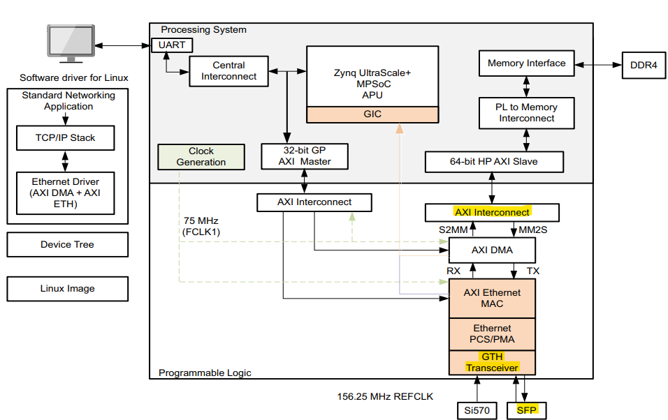
The 10G PL Ethernet Design shown below uses the gigabit transceiver on PL to make a link and the ethernet subsystem itself implements MAC with Physical Coding Sublayer(PCS) and Physical Media Attachment(PMA) layers which are part of PHY, unlike the GEM controllers in the PS.
JESD Standard
The JESD204B interface standard supports the high bandwidth necessary for leading high-performance, high speed and multi-channel applications while reducing the number of digital IOs needed and thus easing board layout. Very high-speed ADCs that would have previously required a complex interface design using a large number of FPGA IO are now implemented with just a few pins.
These have extensive applications in Wireless, SDR and Radar applications where ADCs/DACs are crucial and timing critical sections. A lot of high-speed ADCs like AD9250 come with this protocol interface built-in and on the other side, JESD PHY IP can be implemented on the FPGA PL to make a link through its I/O bank. One special requirement is that it needs a common clock synchronization which you may observe in the below block diagrams.
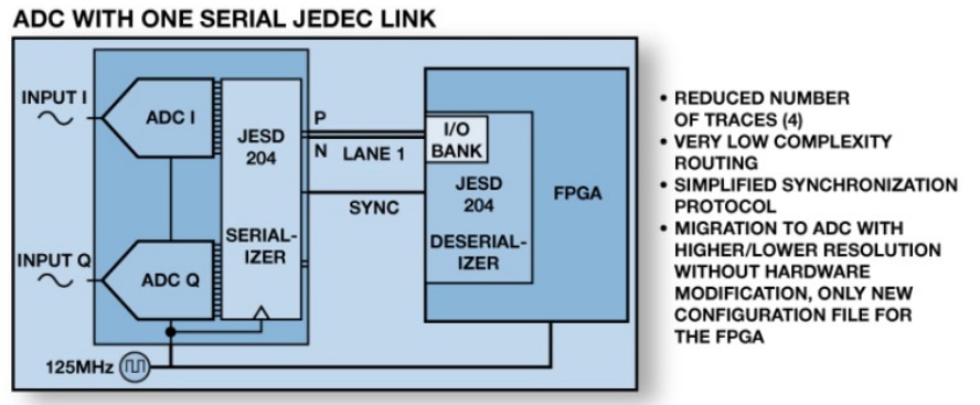
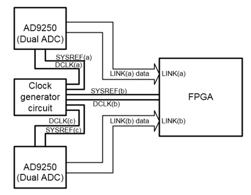
The AMD-Xilinx LogiCORE IP JESD204 PHY core implements a JESD204B physical interface to simplify sharing serial transceiver channels between transmit and receive cores. There are 3 subclasses in this standard and all are supported by this IP. More details regarding subclasses in JESD204B Survival Guide (analog.com)
Further, I am exploring the NEON coprocessor available on Zynq 7000 SoC coupled with a Cortex A9 processor. This is an interesting AppNote on this topic xapp1206-boost-sw-performance-zynq7soc-w-neon.pdf • Viewer • AMD Adaptive Computing Documentation Portal (xilinx.com)
Thanks for reading through. I am now in the process of reading about these protocols and standards along with trying out the NEON coprocessor example implementation in the MiniZed board and Vitis platform. I am sure some of the community members would have worked on some of these, and do share what you think and if any experiences working around these high-speed interfaces.
