


Hey guys,
Hope this new year brings luck and fortune to everyone!
ZynqHW_2017_4_lab_1_v11 :
So I would just cover briefly Lab 1 :
- Guides to setup a new project. I didn't like the fact Avnet is forcing it's users to select target language as VHDL. Would have been great if they could leave the decision up to the reader. So ignoring this particular instruction , I went ahead with Verilog.
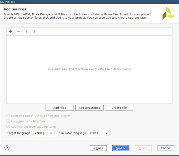
2. After selecting the correct target device, a new Zynq project was created
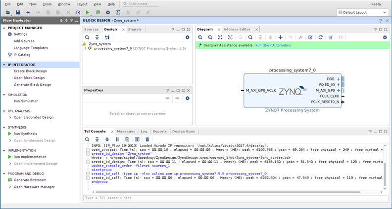
3. One of the fundamental tools in Vivado is the Block Design. There was no such tool in the Xilinx ISE. So after adding the Zynq IP to the block design, a few pins were made external (DDR and Fixed_IO). Final block design looks like this :
Really happy with the little diagrams they have put in every step of the manual. It increases the length and complexity of the lab and I think for someone who is starting with Vivado from scratch it is pretty comprehensive.
Not to happy with the layout though. A few sections I think were unnecessary were being covered in the lab. This could easily be a six to seven page lab manual rather than being an eighteen page one. A simpler version could be drafted for this lab, just containing the steps that are needed to be performed and the reason behind it. I feel these topic aren't required : Lab Setup, Lab Instruction Notes, Technical Support, Lab Overview and Exploring Further.
So that briefly covers Lab 1.
ZynqHW_2017_4_lab_2_v12 :
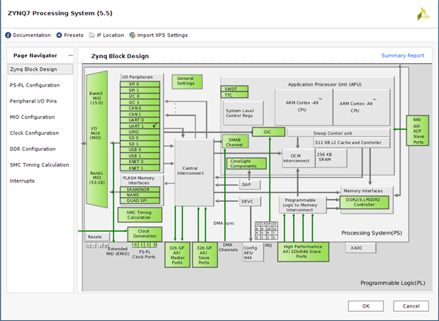
In lab 2, experiment 2 there is a talk of the DDR3 bus. Now the DDR stands for Double Data Rate, which is basically a data transfer protocol occurring at each clock edge (that is : both posedge and negedge). The 3 suffix implies that the memory controller must wait three clock cycles until data is delivered after a request is made. The different steps for DRAM training is explained in UG585, Section 10.6.9 . Now to understand the "DQS line" the DDR configuration has been talking about, this github page is pretty useful : Understanding DDR Memory - Github . In a nutshell, DQS is just the "Data Line Strobe" and it is basically used as an alignment (reference) signal for the Clock and the Data lines of the DDR controller. The Zynq block design looks like this :
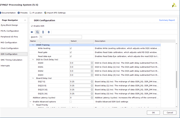
The final part of experiment 2 talks about adding a few delays to "DQS to Clock" and "Board". Now, from what I've learnt : "Never mess with the auto-generated complicated stuff. Especially in Vivado", I will not change any delay values. I know I sound stupid, but to me it just looks like Avnet wants complicate this lab further (why am I so smart ).
).
Onto the most time consuming task in this lab. Getting SDK to work on Ubuntu (lol). After two days of head banging, I would highly recommend everyone to run SDK on Windows. If however you do want to descend into this madness :
- Please do remember to add the following paths to Xilinx SDK in Linux :
/usr/lib/gcc/x86_64-linux-gnu/7/includeand/usr/include. Eclipse does not add the gcc header files path for you :< - Make sure you have the FTDI drivers installed (use
dmesg | tty FTDIto check) - SDK terminal crashes the SDK environment when used (that is to say, when a serial output is being printed).
- \r (carriage return) I think acts funny on Minicom. Not sure about this point though.
So the final result of the "Hello World " came out to be like this :

Please note I did fix up the DQS to clock delay but still no luck. Lab 3 looks like a DMA experiment, so we could see the results then  .
.
The Arch linux setup would be put up as an extra section hopefully by next blog or the next to next one. I have a bloody slow internet connection.
Github link : My git repo for Path to Programmable

