


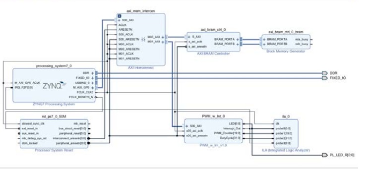
You may remember when we left off, we removed the JTAG interface from our board design, but we left the PWM module and the Logic Analyzer, so the Block Design looked like this:
and I said something about next lab we would do some more TCL scripting and I guessed it would be about removing some IP that we added. BOY WAS I EVER WRONG.
They had us open Vivado, go to the TCL console, change directories into the support directory for lab 9 and type:
source ./lab9.tcl
what that does is execute the TCL script and perform all the commands in the file. I was pleased with myself because you have 2 options when you do this, start from your continuously built labs, and execute the script against your code/project base, or delete your stuff and start over using a zip file of where you should be. It said in the lab that if you encounter errors, you should start over using their zip files. I had no errors, so obviously I must have followed all previous lab directions correctly.
Now this TCL script they had us run was 678 lines long, that includes comments, but it was no doubt a big file. As it was running I saw the above diagram turn into this:
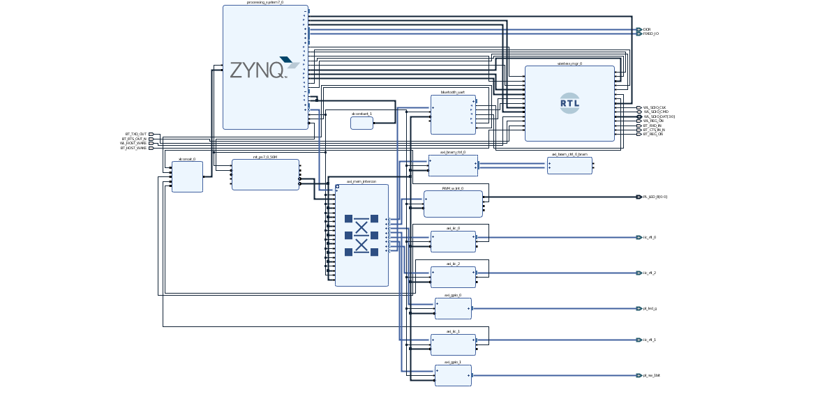
Now that's a little hard to read, so I'll also include the annotated one from the course materials :

They created all of that with TCL commands. And at the end of the script they saved the project, ran the synthesis and implementaion and generated the bitstream for the project. The say it can take anywhere from 15-40 minutes to execute this step. I didn't time it, but I'd estimate I was in the 15-20 minute range, maybe quicker, it didn't seem that long.
Now why would you want to do your design in TCL?
1) You can easily duplicate your design and pass it around, it eliminates computer specific repositories, few issues between various computers and operating systems.
2) It's pretty fast
3) You can customize your finished design easily, for instance re-targeting to a different device.
OK. At this point the lab ended. The final step was to review a few of the files that were generated, then to Export the hardware design for delivery to the Software Team. Which I assume is me when I start Module 2 of the training. Which is supposed to cover the SW development aspect of the MiniZed hardware.
In closing, I'd have to say the Modules were not difficult. I understood everything I was doing and the steps were explained very well. But this is not a course for a total newcomer to take and at the end proclaim "I am a programmable logic master." No, it's far from that, it definitely provided information on the building blocks needed, and it scratched the surface.
I've taken a few 1-2 day seminars in my time from various vendors demonstrating how to use some new hardware or SDK that they've released and this training reminded me of that type of experience. I could easily see this being 2 days of classroom training. With Day 1 going through lab 5, then day 2 consisting of labs 6-9. It was a great experience and I thank Element 14, Avnet, and Xilinx for the experience.
Look forward to my continuing trials as I embark on the second half of this course.
Top Comments