element14 Community
element14 Community
    Register Log In
  • Site
  • Search
  • Log In Register
  • Community Hub
    Community Hub
    • What's New on element14
    • Feedback and Support
    • Benefits of Membership
    • Personal Blogs
    • Members Area
    • Achievement Levels
  • Learn
    Learn
    • Ask an Expert
    • eBooks
    • element14 presents
    • Learning Center
    • Tech Spotlight
    • STEM Academy
    • Webinars, Training and Events
    • Learning Groups
  • Technologies
    Technologies
    • 3D Printing
    • FPGA
    • Industrial Automation
    • Internet of Things
    • Power & Energy
    • Sensors
    • Technology Groups
  • Challenges & Projects
    Challenges & Projects
    • Design Challenges
    • element14 presents Projects
    • Project14
    • Arduino Projects
    • Raspberry Pi Projects
    • Project Groups
  • Products
    Products
    • Arduino
    • Avnet Boards Community
    • Dev Tools
    • Manufacturers
    • Multicomp Pro
    • Product Groups
    • Raspberry Pi
    • RoadTests & Reviews
  • Store
    Store
    • Visit Your Store
    • Choose another store...
      • Europe
      •  Austria (German)
      •  Belgium (Dutch, French)
      •  Bulgaria (Bulgarian)
      •  Czech Republic (Czech)
      •  Denmark (Danish)
      •  Estonia (Estonian)
      •  Finland (Finnish)
      •  France (French)
      •  Germany (German)
      •  Hungary (Hungarian)
      •  Ireland
      •  Israel
      •  Italy (Italian)
      •  Latvia (Latvian)
      •  
      •  Lithuania (Lithuanian)
      •  Netherlands (Dutch)
      •  Norway (Norwegian)
      •  Poland (Polish)
      •  Portugal (Portuguese)
      •  Romania (Romanian)
      •  Russia (Russian)
      •  Slovakia (Slovak)
      •  Slovenia (Slovenian)
      •  Spain (Spanish)
      •  Sweden (Swedish)
      •  Switzerland(German, French)
      •  Turkey (Turkish)
      •  United Kingdom
      • Asia Pacific
      •  Australia
      •  China
      •  Hong Kong
      •  India
      •  Korea (Korean)
      •  Malaysia
      •  New Zealand
      •  Philippines
      •  Singapore
      •  Taiwan
      •  Thailand (Thai)
      • Americas
      •  Brazil (Portuguese)
      •  Canada
      •  Mexico (Spanish)
      •  United States
      Can't find the country/region you're looking for? Visit our export site or find a local distributor.
  • Translate
  • Profile
  • Settings
Path to Programmable
  • Challenges & Projects
  • Design Challenges
  • Path to Programmable
  • More
  • Cancel
Path to Programmable
Blog Labs 5 & 6
  • Blog
  • Forum
  • Documents
  • Polls
  • Files
  • Events
  • Mentions
  • Sub-Groups
  • Tags
  • More
  • Cancel
  • New
  • Share
  • More
  • Cancel
Group Actions
  • Group RSS
  • More
  • Cancel
Engagement
  • Author Author: mconners
  • Date Created: 3 Nov 2018 4:25 PM Date Created
  • Views 747 views
  • Likes 6 likes
  • Comments 5 comments
Related
Recommended

Labs 5 & 6

mconners
mconners
3 Nov 2018

Finally starting to access the PL


I grouped labs 5 & 6 together because they really are 2 parts of a single lab. Lab 5 was adding a Block Ram to the Processing System using the AXI Interconnect System, Lab 6 was actually Programming the FPGA to create the IP, and the second half was compiling a program and installing it on the CPU to execute some DMA tests, record the timings, and calculate the speed savings using Interrupt DMA. One of the enlightening things about this lab was seeing all of the different types of IP designs they provide for you. I'm not sure of the exact number, but they have FFT and DFT blocks, FIFO's, Ethernet Blocks, Video Frame Buffers, Processor Cores, and much, much more.


image


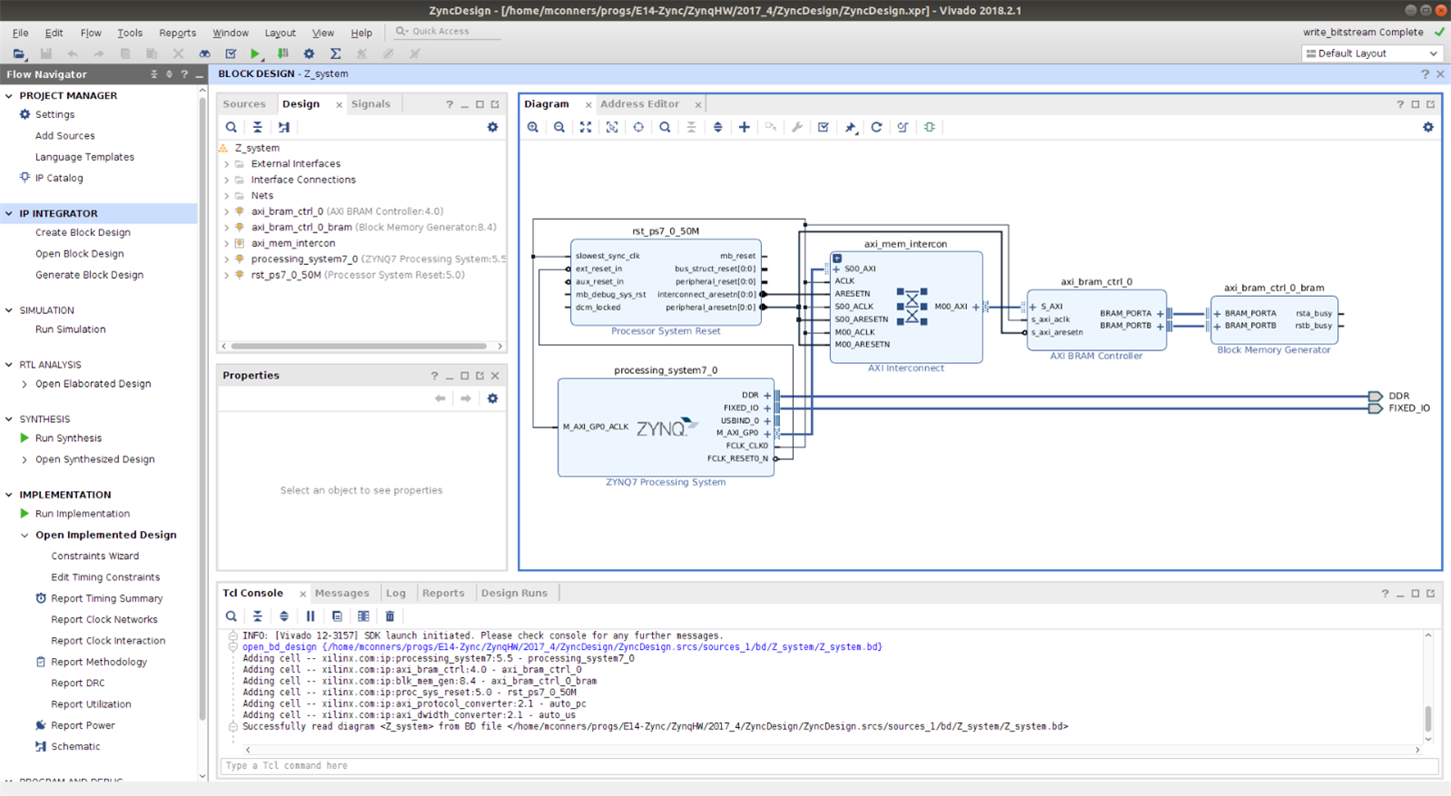
If you look at some of my earlier blogs, you may remember that the above diagram only contained the ZYNQ7 Processing System. In the lab we added the Reset Block, the AXI Interconnect, the BRAM Controller, and the Block Memory Generator. It's a lot of steps so I won't go through them here, but it's not a difficult process to add each of the components. I did not have to draw the interconnect lines, it did that when I added each of the blocks. So that was nice. It also took care of arranging the blocks for me.


image


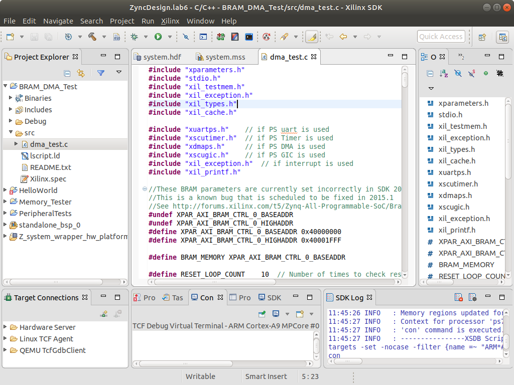
The above is a screenshot of the SDK. They had a pre written program to exercise the Block Memory they had us add. We did make use of a new button this time. Right below the help link, there is a button with a red arrow and 3 green boxes. We clicked on that to program the FPGA. After that we hooked up the console below. Flashed the processor, and exercised the newly added IP.


image


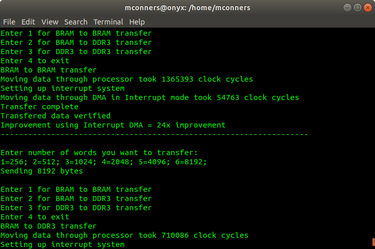
In the above example, I had chosen an 8192 block size for a DMA transfer of BRAM to BRAM, which resulted in 24x improvement over having the CPU copy the data.


image


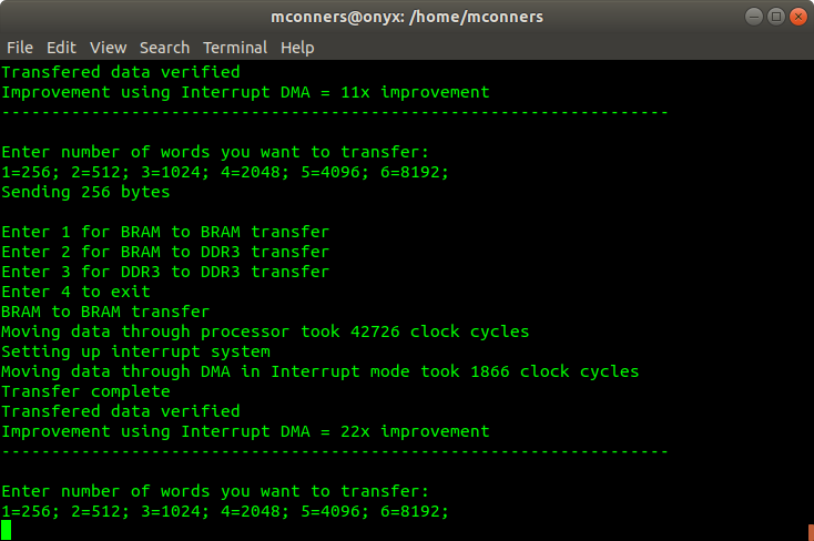
The above screen capture is more of the same. I pretty much tried all the combinations.


That's it for Labs 5 & 6. Really just a baby step that we will build on. Lab 7 is about creating Custom IP so that should be a bit more interesting.


I am enjoying this, and I'm glad I'm remembering what we did in previous labs, so their technique  is working. The material and exercises are not particularly difficult, but the ZYNC7 processor is a very complex device. There are a lot of possible configurations and uses so we'll see where this goes.


That's all for now. If you have questions, feel free to ask.

  • Sign in to reply

Top Comments

  • mconners
    mconners over 6 years ago in reply to DAB +2
    Hey DAB, Each lab is preceded by a video, along with a set of slides. I've been to a number of 1-2 day seminars put on by manufacturers like ST, and this seems very comparable. One of the testers commented…
  • shabaz
    shabaz over 6 years ago in reply to mconners +2
    Hi Mike, I totally agree with you, the pace is easy to move at! It's great to see what you've worked on in these labs, I still have to do them. Very cool that the labs will take us into using these other…
  • rscasny
    rscasny over 6 years ago in reply to aspork42 +2
    James, Both you and Shabaz bring up great points regarding what is or is not included in the module, etc. I think this addresses the bigger question about curriculum development: should it cover everything…
Parents
  • DAB
    DAB over 6 years ago

    Nice update Mike.


    I am curious, how much time did you spend reading the material and then how much time did it take you to implement each lab?


    DAB

    • Cancel
    • Vote Up +1 Vote Down
    • Sign in to reply
    • More
    • Cancel
  • mconners
    mconners over 6 years ago in reply to DAB

    Hey DAB,


    Each lab is preceded by a video, along with a set of slides. I've been to a number of 1-2 day seminars put on by manufacturers like ST, and this seems very comparable. One of the testers commented that it seems like a semesters worth of material, but to be honest, what we have been provided so far seems like it would be a 2 day seminar by Avnet or Xilinx. Not that that is bad in anyway. Lab 5 seemed like it would be the last lab of Day 1 and lab 6 seems like it would be the follow on the next day. I looked at what shabaz wrote up and I have to say he went above an beyond the info that is supplied in the training and did a fantastic job. I've debated internally about whether to go into that depth, or to simply blog about each lesson as it's presented and then supply a detailed write up of what I've learned at the end. So, to ultimately answer your question, I'd say about 30 minutes of lecture, followed by 30 minutes of lab, followed by about 30-45 minute of review and documentation on my part at the end.


    Mike

    • Cancel
    • Vote Up +2 Vote Down
    • Sign in to reply
    • More
    • Cancel
Comment
  • mconners
    mconners over 6 years ago in reply to DAB

    Hey DAB,


    Each lab is preceded by a video, along with a set of slides. I've been to a number of 1-2 day seminars put on by manufacturers like ST, and this seems very comparable. One of the testers commented that it seems like a semesters worth of material, but to be honest, what we have been provided so far seems like it would be a 2 day seminar by Avnet or Xilinx. Not that that is bad in anyway. Lab 5 seemed like it would be the last lab of Day 1 and lab 6 seems like it would be the follow on the next day. I looked at what shabaz wrote up and I have to say he went above an beyond the info that is supplied in the training and did a fantastic job. I've debated internally about whether to go into that depth, or to simply blog about each lesson as it's presented and then supply a detailed write up of what I've learned at the end. So, to ultimately answer your question, I'd say about 30 minutes of lecture, followed by 30 minutes of lab, followed by about 30-45 minute of review and documentation on my part at the end.


    Mike

    • Cancel
    • Vote Up +2 Vote Down
    • Sign in to reply
    • More
    • Cancel
Children
  • shabaz
    shabaz over 6 years ago in reply to mconners

    Hi Mike,


    I totally agree with you, the pace is easy to move at! It's great to see what you've worked on in these labs, I still have to do them. Very cool that the labs will take us into using these other bits of IP. I was not sure what to blog either, so figured that since I'm a novice I might take it slower. I reckon it's really helpful for readers that there are different speeds of information and different levels of experience.. I always like to read several textbooks if I'm learning something new.. and I suspect that anyone who reads these blogs might do the same. It's just like having many books : ) I'll be interested to compare your output screenshots above with what I get when I reach this point.. curious to see the same cycle counts : )

    • Cancel
    • Vote Up +2 Vote Down
    • Sign in to reply
    • More
    • Cancel
element14 Community

element14 is the first online community specifically for engineers. Connect with your peers and get expert answers to your questions.

  • Members
  • Learn
  • Technologies
  • Challenges & Projects
  • Products
  • Store
  • About Us
  • Feedback & Support
  • FAQs
  • Terms of Use
  • Privacy Policy
  • Legal and Copyright Notices
  • Sitemap
  • Cookies

An Avnet Company © 2025 Premier Farnell Limited. All Rights Reserved.

Premier Farnell Ltd, registered in England and Wales (no 00876412), registered office: Farnell House, Forge Lane, Leeds LS12 2NE.

ICP 备案号 10220084.

Follow element14

  • X
  • Facebook
  • linkedin
  • YouTube