


About:
Through Avnet, Xilinx and Element14, a training program to learn about the Zynq 7000 platform which is System On Chip combining an FPGA with an ARM processor. This comes to the students as complete development board packed with goodies like a wireless chip from MuRata (BT/BTLE/WIFI), 8GB Flash memory, onboard RAM, USB to JTAG (JTAG programmable over USB), Arduino-style headers (3.3V compatible only), Microphone, Bi-Color LED, and two additional expansion ports.
See all blog posts for this training here.
Lab 8 - Debugging methods and techniques
Lab 8 focuses on the different way that we can debug the FPGA hardware. In the last lab we imported an example program for creating a PWM controller with interrupt capabilities. In this lesson, we pick up from where that left off, then integrate the PS (software) to give a command line front-end to the controller. The software portion prompts the user for input from 0-9; then it reports this to the PL (hardware) the updated period value.
The hardware portion (added in Vivado then exported as a board support package for the SDK) responds by counting the input clock cycles and setting the output pin high or low according to the duty cycle.
Debugging through the computer can be done one of three ways:
- ILA (Integrated Logic Analyser)
- VIO (Vivado Input/Output)
- JTAG (JTAG2AXI)
For starters, we first load the MiniZed with the program and debug using a 4th method - an oscilloscope. As noted above, the user interface is a command line through Putty. I hook my scope up to pin header A4 + GND (Arduino Analog 4) as per the schematics. The A4 pin is directly connected to the PFGA output from the PWM controller.
Here are the relevant portions of the schematic showing the pinout:
| {gallery:autoplay=false} My Gallery Title |
|---|
1
|
2
|


Here are the scope traces for the different levels in the PWM controller.
| {gallery} Lab 8 Lesson 1 |
|---|
Level 0 Scope trace with Brightness 0 selected |
Level 1 Scope trace with Brightness 1 selected |
Level 2 Scope trace with Brightness 2 selected |
Level 3 Scope trace with Brightness 3 selected |
Level 4 Scope trace with Brightness 4 selected |
Level 5 Scope trace with Brightness 5 selected |
Level 6 Scope trace with Brightness 6 selected |
Level 7 Scope trace with Brightness 7 selected |
Level 8 Scope trace with Brightness 8 selected |
Level 9 Scope trace with Brightness level 9 selected |

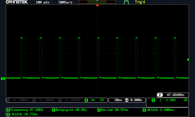


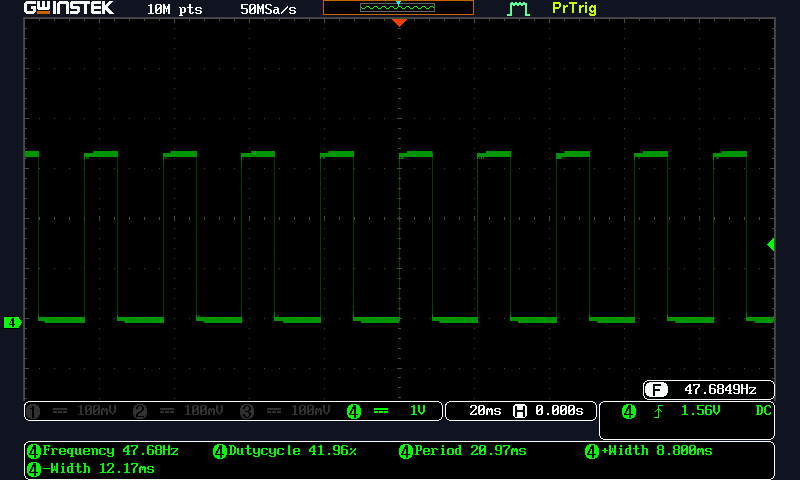
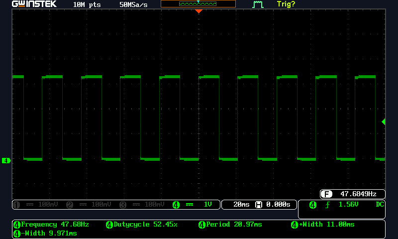
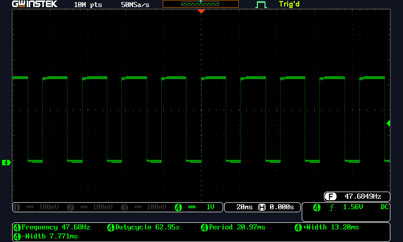


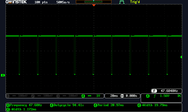
Here is a quick video showing the results as they appeared on the scope. The [slowish] ~50 Hz frequency can easily be seen in the scope traces as they update.
Debug with the ILA
The Integrated Logic Analizer (ILA) is a built-in feature in Vivado. This was added at the block design to allow reading certain signals. We can see below (in orange) how it has been wired (back in a previous lesson) to "probe" the LED output, PWM Counter output, and Duty Cycle output from the PWM logic block.

The ILA is found within Vivado's "Hardware manager". We configure the trigger to hit when the interrupt pin has a "low-to-high" transition by selecting "R" from the "Value" pull-down menu in our trigger setup. We arm the logic analyzer just like a regular scope or logic analyzer and it waits for the trigger to occur.
The program call for the interrupt to go HIGH any time an invalid option is selected by the user. In this program's case, the invalid data is found by the FPGA code (PL) and not the software (PS). The captured results are shown below.

We can see from this capture that the Interrupt occurred one PWM Counter cycle after the Duty Cycle changed. The Duty cycle shows 770,000 changing to 5,720,000. That means that I was on a Brightness of 7 and I pressed some other key on the keyboard which wasn't numerical between 0 and 9. So the interrupt happened one PWM cycle after the invalid data was sent. If I'm understanding the code correctly, one PWM Cycle would be as follows: 50 MHz clock / 20 (clock divisor) = 2,500,000 clock cycles. That works out to 0.05 seconds for the interrupt to take effect. Unfortunately the logic analyzer is limited to a capture depth of 1024 samples which isn't very much. The interrupt may be handled much faster than that.
Debug with JTAG2AXI
With this method, we can somewhat hijack command of the PWM by sending commands through a different AXI Interconnect. So instead of using the software-based frontend, we can us the TCL command line to manually push down values into our FPGA program. This is kinda-sorta-but-not-really like a "man in the middle" attack - the downstream nodes don't really know where the upstream message is coming from; they respond the same way. This is also somewhat similar to how MQTT works - A host "listens" to a topic and responds every time it is required. It doesn't know who posts to the topic, it responds the same no matter what.
In this figure - we can see how the Zync PS (Software) is using the first AXI channel into the AXI Interconnect; which then points down to the PWM controller.
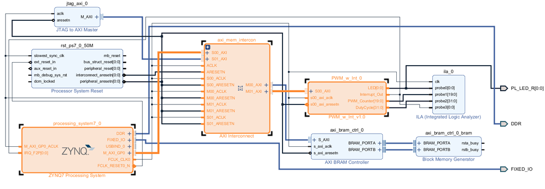
Now; with the second debug option we are able to see how the JTAG To AXI uses a second AXI channel into the AXI Interconnect.

The downstream PWM controller still has the same connection to the AXI Interconnect; so it continues to respond the same way. One major purpose for doing debugging this way has to do with development cycles. The embedded programmer may not yet have a program from the Software team; but is still ready to test. This also makes it easier to force certain values and scenarios to test specific use cases easily.
This is a two-part process. We have to create a string which contains the memory address and new value and a few other parameters; then we have to send a second command to execute the string.
The two strings from the example are as follows:
create_hw_axi_txn write_txn [get_hw_axis hw_axi_1] -type WRITE -address 43C00000 -len 1 -data 000A1220
run_hw_axi [get_hw_axi_txns write_txn]
The "-data" is the actual brightness level that we send down to the PWM controller. It was created using a base address of 43C0_0000 which we see in the command.
We can update the Data with the command:
set_property DATA 000FFFFF [get_hw_axi_txns write_txn]
run_hw_axi [get_hw_axi_txns write_txn]
As with before; this is a two-part process. One to store the updated string and a second to execute it.
Both the ILA and my oscilliscope verified that once the "run" command was sent in the TCL interface; the PWM controller responded correctly. The Serial interface continued to update as well; which seemed a bit odd. I'm not sure how Vivado and PuTTY are able to share the resource (COM8) so nicely...
Another interesting thing is that we can dial in the PWM more accurately this way. I can manually set the data rather than using the PuTTY command line. I could get duty cycles as low as 0.02%. The upper limit was still a duty cycle of 94.41%; which was verified by sending a value 000F 1B30 which is 990,000 in decimal; which matches the PL program as the maximum allowable input value. See the image above with the Brightness of 9.


There is also the ability to write directly to the BRAM (which was covered in a previous post). This is a two-part process as before. The first step is to create the command; and the second is to execute it. We expiremnet by writing to BRAM; then reading it back with a different Read command.
Here is the address map showing address 0x4000_0000 as the base address of the BRAM; as well as the address of the PWM controller.

Here are the sample commands that I ran to read; then write; then read back to verify. My commands in the TCL console show as BLUE below.

The last portion of the lesson is to remove the JTAG to AXI Interconnect. This is done since it would be the last thing before a project is made final. The JTAG to AXI wouldn't be required in a final product according to the lessons. (Side note: I've been in many-a-meeting arguing over what is really required in the final product...)
Project update:
Its been a while since I've done one of these. I have my parts list picked out to create a line follower. The more I get into this training program; the more it seems that I have a lot left to learn! I still plan on completing a project with the MiniZed but will need to reign in my ambitions before I get too carried away. I have one lesson left to go in the first training session and can't wait to really get working on my own and find my own way around with this cool device 
Until next time!
-

DAB
-
Cancel
-
Vote Up
0
Vote Down
-
-
Sign in to reply
-
More
-
Cancel
Comment-

DAB
-
Cancel
-
Vote Up
0
Vote Down
-
-
Sign in to reply
-
More
-
Cancel
Children