


(Complete list of all blog entries in this series)
This is probably the second-to-last article about my project, on the last day I will try to upload a video showing how it all works together.
On the weekend I went ahead and finally put together all the parts that lived on the different breakout boards for the last few months. I had ordered some new smaller batteries in the meantime, so I went ahead and looked for a new enclosure too.
But the first task was to mount the ADXL board on to of the PSoC BLE board, together with the UI elements I needed (a LED and one push button):
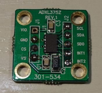
I used my Proxxon IBS/E50 to cut the PCB down so only the area with the components on it was left. It meant that the silk screen was gone, but I made this picture for future reference.
When you look closely, you can see that the holes in both rows are not matched against each other - they are shifted by 50mil. That means you cannot mount it directly on a perfboard, only one row can be done this way. Thats quite a shame - for a breakout board I would expect using standard mounting pattern.
Before soldering the ADXL on a Perfboard, I prepared the PSoC BLE module board. I had already removed the existing female headers, and now added male headers for the pins that are needed:
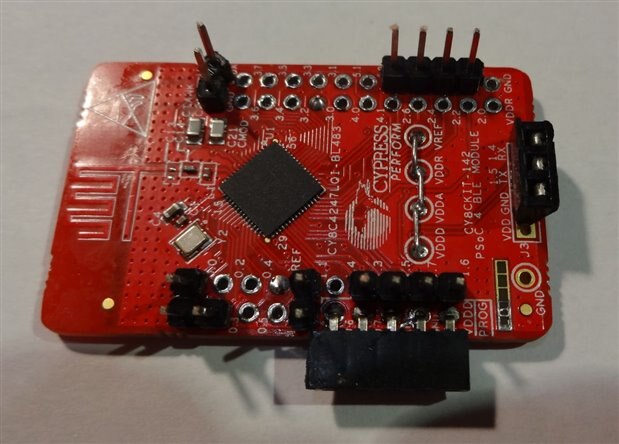
The two female headers are for the Miniprog3 and the serial debugging output.
Cypress did the same mistake as Analog Devices - using non-standard pin layouts. Both headers rows are not spaced in a 100mil grid (the headers itself are, but their distances isn't). So I needed to solder in the pins sideways to fit the perf boards in top. Same is true for the supply pins (Vddd, Vdda, Vddr). Why do manufacturers do this?
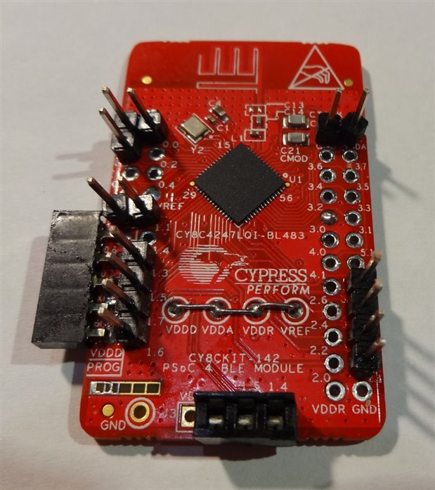
Next comes the perf boards on top of the BLE module, and the ADXL on top of that:

If it would not be for the button, I would have mounted the ADXL board on the other side of the perf board to save some vertical space.
After soldering everything together I tested a first "blinky" example to se whether everything was OK. Turned out it wasn't everytime the MiniProg powered the board it would disappear from the device manager. The mistake was a simple one - I had accidentally shorted Vdd to GND 
Having solved that it now looked fine and I proceeded with programming my SkiMonitor program to check that the ADXL375 was still usable.
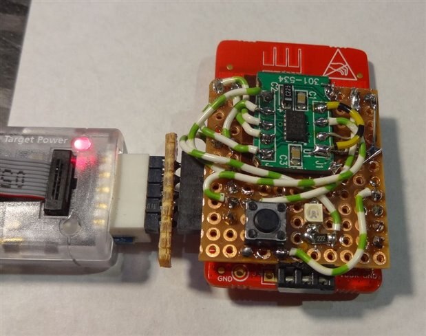
Apart from having swapped the two interrupt lines (INT1 and INT2) everything was fine, and that change could be solved in the schematic editor of PSoC Creator.
So time had come to put everything into the enclosure. It started with the wireless charger and the battery:
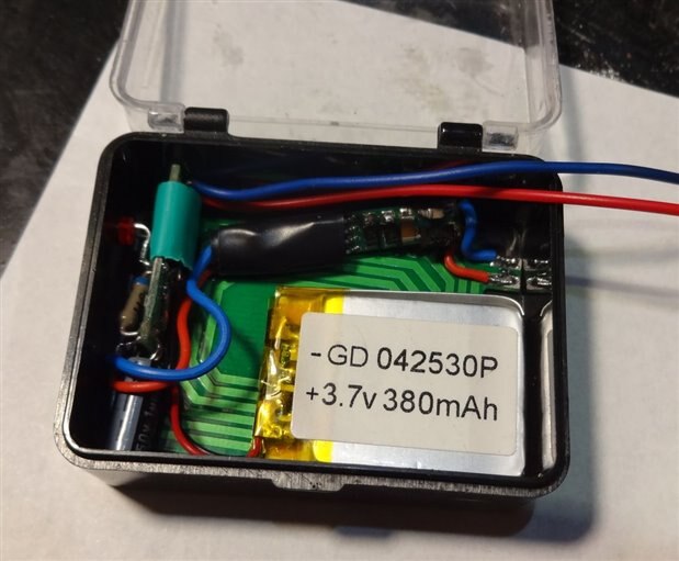
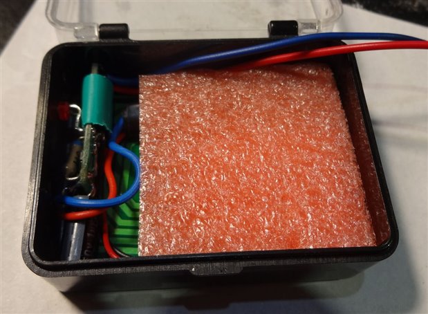
The receiver coil goes to the bottom, the battery above it. To the top is the receiver circuit, on the left the battery charger and the LDO (providing 2.5V). To hold everything in place I added some foam above the battery:
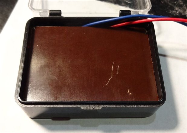
and then some plastic sheet as insulation:
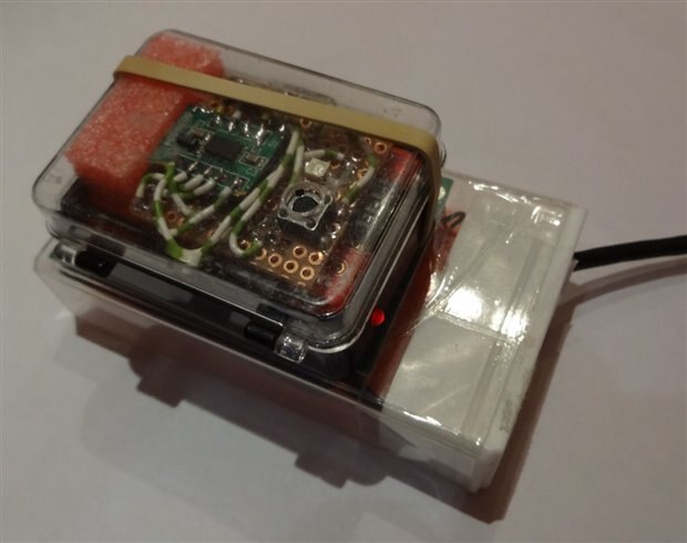
Then the PSoC BLE board with the rest of the circuit goes on top of it. The lid of the enclosure now holds the PCB in place, but I needed a small hole for the button (which is used to start BLE pairing).
For this picture I placed the Ski monitor on top of the wireless charger transmitter, the small LED on the right signals the charging process.
With that the prototype is finished from the hardware side. For now there is still some work on the software side that could improve the feature-set and the usability. And I will do further work on a PCB that could incorporate the full circuit on one PCB (while not being larger than the PSoC4 module board).

