element14 Community
element14 Community
    Register Log In
  • Site
  • Search
  • Log In Register
  • Community Hub
    Community Hub
    • What's New on element14
    • Feedback and Support
    • Benefits of Membership
    • Personal Blogs
    • Members Area
    • Achievement Levels
  • Learn
    Learn
    • Ask an Expert
    • eBooks
    • element14 presents
    • Learning Center
    • Tech Spotlight
    • STEM Academy
    • Webinars, Training and Events
    • Learning Groups
  • Technologies
    Technologies
    • 3D Printing
    • FPGA
    • Industrial Automation
    • Internet of Things
    • Power & Energy
    • Sensors
    • Technology Groups
  • Challenges & Projects
    Challenges & Projects
    • Design Challenges
    • element14 presents Projects
    • Project14
    • Arduino Projects
    • Raspberry Pi Projects
    • Project Groups
  • Products and Partners
    Products and Partners
    • Arduino
    • Avnet & Tria Boards Community
    • Dev Tools
    • Manufacturers
    • Multicomp Pro
    • Product Groups
    • Raspberry Pi
    • RoadTests & Reviews
  • About Us
    About the element14 Community
  • Store
    Store
    • Visit Your Store
    • Choose another store...
      • Europe
      •  Austria (German)
      •  Belgium (Dutch, French)
      •  Bulgaria (Bulgarian)
      •  Czech Republic (Czech)
      •  Denmark (Danish)
      •  Estonia (Estonian)
      •  Finland (Finnish)
      •  France (French)
      •  Germany (German)
      •  Hungary (Hungarian)
      •  Ireland
      •  Israel
      •  Italy (Italian)
      •  Latvia (Latvian)
      •  
      •  Lithuania (Lithuanian)
      •  Netherlands (Dutch)
      •  Norway (Norwegian)
      •  Poland (Polish)
      •  Portugal (Portuguese)
      •  Romania (Romanian)
      •  Russia (Russian)
      •  Slovakia (Slovak)
      •  Slovenia (Slovenian)
      •  Spain (Spanish)
      •  Sweden (Swedish)
      •  Switzerland(German, French)
      •  Turkey (Turkish)
      •  United Kingdom
      • Asia Pacific
      •  Australia
      •  China
      •  Hong Kong
      •  India
      •  Japan
      •  Korea (Korean)
      •  Malaysia
      •  New Zealand
      •  Philippines
      •  Singapore
      •  Taiwan
      •  Thailand (Thai)
      •  Vietnam
      • Americas
      •  Brazil (Portuguese)
      •  Canada
      •  Mexico (Spanish)
      •  United States
      Can't find the country/region you're looking for? Visit our export site or find a local distributor.
  • Translate
  • Profile
  • Settings
element14's The Ben Heck Show
  • Challenges & Projects
  • element14 presents
  • element14's The Ben Heck Show
  • More
  • Cancel
element14's The Ben Heck Show
Forum Etching circuit boarda
  • Blog
  • Forum
  • Documents
  • Polls
  • Files
  • Members
  • Mentions
  • Sub-Groups
  • Tags
  • More
  • Cancel
  • New
Join element14's The Ben Heck Show to participate - click to join for free!
Actions
  • Share
  • More
  • Cancel
Forum Thread Details
  • Replies 16 replies
  • Subscribers 33 subscribers
  • Views 2609 views
  • Users 0 members are here
Related

Etching circuit boarda

jds123
jds123 over 13 years ago

I've been thinking about etching my own boards for awhile now, and I am wondering about a few things.

  1. Which is better for the traces, UV paint boards or LaserJet Printer boards?
  2. Are there alternatives to LaserJet Printing for boards?
  3. Is it cost efficient?
  4. Where can I get the board to etch?
  • Sign in to reply
  • Cancel

Top Replies

  • shabaz
    shabaz over 13 years ago in reply to jds123 +1
    I havn't done it in a while, but from experience, for good results, a photo-sensitive method is required where the image is on a transparent sheet. Other methods of transferring the pattern to the board…
  • benheck
    benheck over 13 years ago +1
    I haven't done this sort of thing before, but I wish you luck! I might try to squeeze a CNC PCB milling machine into Season 3
Parents
  • benheck
    benheck over 13 years ago

    I haven't done this sort of thing before, but I wish you luck!


    I might try to squeeze a CNC PCB milling machine into Season 3 image

    • Cancel
    • Vote Up +1 Vote Down
    • Sign in to reply
    • Cancel
  • e14 Contributor
    e14 Contributor over 13 years ago in reply to benheck

    That would be cool Ben. I've won a prize but then would really  really want to win that one image  Hope you can do that and make plans availiable.


    I've tried toner method and hadnt had success with that. Tried with magazines, special paper and laminator, iron ugh.   Going to try photoresist method next and use the presensitized boards.  Seen trying to get spray evenly can be hard on some youtube videos.   I've tried using protoboards but a bit of a hassle for me.  Though might try the veraboard that have some traces that u just break as needed. They might be eaiser than trying to solder bridge everything and wiring point to point.


    For buying regular copper clad board for the toner method, I bought off of ebay from this person http://www.ebay.com/itm/120664289524?var=420018556386&ssPageName=STRK:MEWAX:IT&_trksid=p3984.m1423.l2649.  Seemed to have good pricing and cut to size for free to fit what the free Eagle cad software can use.


    For presensitized was thinking of ordering from here for their starting kit.  http://www.circuitspecialists.com/416k.html  Order some stuff from them before and was good quality. Seem to have best price for this kit with checking some of the other suppliers.

    • Cancel
    • Vote Up 0 Vote Down
    • Sign in to reply
    • Cancel
  • shabaz
    shabaz over 13 years ago in reply to e14 Contributor

    If you really want to go through the home-made PCB route (I stopped after a while, it was just too much hard work! ; -) and you're pursuing the non-CNC method, then step 1 is to confirm you can create a very opaque image on a transparency, by holding it up to a strong light. If you cannot, you should stop right there - otherwise it is just a wasted attempt at photoresist, chemical etching, etc.

    The opaqueness is really key to a good result. If you can achieve that, then you can create very detailed boards fairly reliably.

    For example, here is a photo showing two PCBs created with a professional photo-plot, but with home exposure and etching. They are both double-sided (with wires linking the holes), and you can see the lower PCB has some fairly fine tracks. It looks oxidized because it is quite old and was not protected. It still works (it was the last board I ever did with home etching). Some people print multiple times over the same transparency, to get it extremely dense. It really depends on the printer and type of plastic sheet. I've used a photocopier in the past (special plastic is required, otherwise it will melt).

    image

    The key point to Stage 2 is to ensure that you're using pre-sensitized boards. The spray-can method works, but it is hard to be consistent from one attempt to the next.

    The key point to the chemical etching stage is to use a warm bath and some occasional agitation. Otherwise, it etches too slow and eats up the thin tracks. There are small heaters in a test-tube-like enclosure that are fairly low cost.

    • Cancel
    • Vote Up 0 Vote Down
    • Sign in to reply
    • Cancel
  • mikemoretti
    mikemoretti over 13 years ago in reply to shabaz

    I'm in the process of designing a PCB that I plan to etch myself.  How do you get the copper ground plane to be separate from the pads and parts that aren't connected to it?  So far, in my board layout, only the wirepads seem to be separated from the ground plane.  Everything else seems to run right into it.  Is there some kind of script I need to run to format this thing for etching?


    Thanks!

    • Cancel
    • Vote Up 0 Vote Down
    • Sign in to reply
    • Cancel
  • shabaz
    shabaz over 13 years ago in reply to mikemoretti

    Hi Mike,


    I'm not sure I understand, you may need to post an image of it.

    Generally, with EAGLE, for a ground plane, all you need to do is route the board (manually or automatically) then

    draw an outline using the 'Polygon' icon, and then  name it the same net name as your ground plane

    (e.g. 'GND'), and then click the strange icon that looks like an 'X with blobs' (when you hover over it,

    it says 'Calculate shortest airwaves'). This will lay a plane around all your existing traces, without touching any except GND.

    image

    • Cancel
    • Vote Up 0 Vote Down
    • Sign in to reply
    • Cancel
  • mikemoretti
    mikemoretti over 13 years ago in reply to shabaz

    Hi,


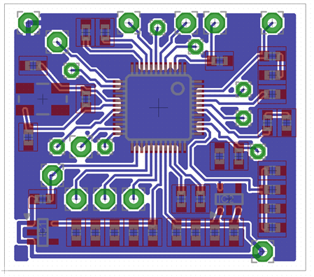
    I did exactly what you mentioned, it lays a plane around them but it touches everything except wirepads.  Here's a picture:


    image

    You see all those smd resistors and caps?  The pads where the routes are touch the ground plane because the ratsnest tool didn't isolate the those pads on them.  Yet it isolated the ones on the wirepads.  It makes no sense to me.  These are standard 0603 resistors and caps I got from the "rcl" library.  Maybe I should've put all my traces on the top layer?


    Thanks!

    • Cancel
    • Vote Up 0 Vote Down
    • Sign in to reply
    • Cancel
  • shabaz
    shabaz over 13 years ago in reply to mikemoretti

    Hi Mike,


    Yes, basically your SMD devices are currently on the top layer (because they are in red), but the traces are on the bottom layer (blue), so they

    are not touching.

    There is a similar problem with the IC, because it is on the top layer, but the tracks are on the bottom layer.

    Ordinarily EAGLE will automatically identify this and won't allow you to do this. Did you draw the schematic first, and then change the yellow airwaves into tracks?

    (If you skip the schematic step, there is a chance for a lot of errors to occur).

    • Cancel
    • Vote Up 0 Vote Down
    • Sign in to reply
    • Cancel
  • mikemoretti
    mikemoretti over 13 years ago in reply to shabaz

    Ahh, I see.  Yeah, I drew the schematic first and then had it generate the board.  Then I manually placed the routes. 


    Now that I've messed around a little more I can see that I will need to put my traces on the Top as you said and it looks like it works perfectly.  Thanks!!!


    I got my instructions for doing this from someone who said I should put my traces on the Bottom...


    -m

    • Cancel
    • Vote Up 0 Vote Down
    • Sign in to reply
    • Cancel
  • shabaz
    shabaz over 13 years ago in reply to mikemoretti

    No problem. Good luck with the board!

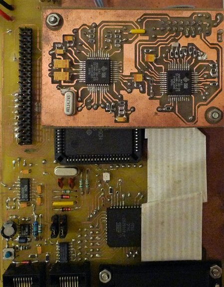
    By the way, since this is going to be a home-etched board and likely single-sided, the green pads will be on top only too, so any wires that you connect will have to be fed through from the bottom of the board and soldered to the top, same as the SMD devices, or perhaps solder in some pins but from the top.

    In the photo in post number 7, I actually had the same problem with the long DIL header you can see at the top-left of the board. What you can't see is that I had to lift the header quite high and solder it from the top side of the board, so actually that header is raised somewhat from the surface of the board. It's rather messy but is fine for a prototype of course.

    The board you can see mounted on screws hasa DIL header soldered from the underside (you can see the parallel row of soldered joints near the top of the board).

    So, home-etching does have some challenges ocassionally, due to the absence of through-hole capability. At the bottom of the large board, you can see near a nut that there are many solder blobs; these were through-hole bits of wire. Again, rather messy but works.

    • Cancel
    • Vote Up 0 Vote Down
    • Sign in to reply
    • Cancel
Reply
  • shabaz
    shabaz over 13 years ago in reply to mikemoretti

    No problem. Good luck with the board!

    By the way, since this is going to be a home-etched board and likely single-sided, the green pads will be on top only too, so any wires that you connect will have to be fed through from the bottom of the board and soldered to the top, same as the SMD devices, or perhaps solder in some pins but from the top.

    In the photo in post number 7, I actually had the same problem with the long DIL header you can see at the top-left of the board. What you can't see is that I had to lift the header quite high and solder it from the top side of the board, so actually that header is raised somewhat from the surface of the board. It's rather messy but is fine for a prototype of course.

    The board you can see mounted on screws hasa DIL header soldered from the underside (you can see the parallel row of soldered joints near the top of the board).

    So, home-etching does have some challenges ocassionally, due to the absence of through-hole capability. At the bottom of the large board, you can see near a nut that there are many solder blobs; these were through-hole bits of wire. Again, rather messy but works.

    • Cancel
    • Vote Up 0 Vote Down
    • Sign in to reply
    • Cancel
Children
  • mikemoretti
    mikemoretti over 13 years ago in reply to shabaz

    Yeah, I had planned to feed the wires through the bottom.  I even have some traces I need to connect by wire because my chip needs 3 separate power voltages on something like 12 different pins and I can't get them all to connect without drilling through and running wires (that's what the smaller holes are for on that board)...


    I notice on your board you either have a huge isolation value or orphans is off (lots of etched away space in the middle of the board around the chips and the things connected to them).  It looks clean.  I may need to do that too depending on how this all comes out (instead of having ground EVERYWHERE).


    Thanks again,

    -m

    • Cancel
    • Vote Up 0 Vote Down
    • Sign in to reply
    • Cancel
  • shabaz
    shabaz over 13 years ago in reply to mikemoretti

    You're right, to be honest that board may not be EAGLE, or may be done by hand. I think I was just trying to save a bit of etchant rather than have a ground plane (possibly the underside may have one if it is dual-layer). It was a very long time ago (I experimented with quite a few CAD packages over the years, but eventually stumbled upon EAGLE from version 4.x and I've been using it ever since (although I do occasionally use some other packages).

    • Cancel
    • Vote Up 0 Vote Down
    • Sign in to reply
    • Cancel
element14 Community

element14 is the first online community specifically for engineers. Connect with your peers and get expert answers to your questions.

  • Members
  • Learn
  • Technologies
  • Challenges & Projects
  • Products
  • Store
  • About Us
  • Feedback & Support
  • FAQs
  • Terms of Use
  • Privacy Policy
  • Legal and Copyright Notices
  • Sitemap
  • Cookies

An Avnet Company © 2026 Premier Farnell Limited. All Rights Reserved.

Premier Farnell Ltd, registered in England and Wales (no 00876412), registered office: Farnell House, Forge Lane, Leeds LS12 2NE.

Follow element14

  • X
  • Facebook
  • linkedin
  • YouTube