


Hey everyone, this is my first post here so apologies if anything is awry with the formatting or layout :)
Project and Background
Recently I have been working on a remote, motorised SDR satellite base station project (coming soon!), using an Arduino Uno Q and an RTL-SDR. As part of this, I have been looking into ways to squeeze as much performance out of my RTL-SDR dongle as is possible. One issue with these dongles is a high noise floor, this is critical for sensitive applications where very small input signals are involved - if the noise floor is too high, then these weak received signals will be unrecoverable or have a very high BER. A very common source of noise in RF circuits is through the supply, USB power is typically quite dirty, especially from cheap devices. It contains high frequency contaminants in the band of interest (10kHz-10MHz) from lots of different circuits, such as switching regulators, clocks or simply from the USB data lines (for example, USB 2.0 high speed, which has a fundamental at 6MHz). Supply noise directly raises the noise floor (since circuits in the RF front end, such as the LNA, mixers, or VCOs do not have an infinite PSRR, which we will cover in more detail later), so one easy improvement to boost the performance of these SDRs might be to filter their supplies.
Filtering of high frequency noise usually takes the form of a lowpass filter, as this provides attenuation for high frequencies (pole). Since we want to supress all noise from DC upwards, a lowpass filter could be designed for this job. The cutoff frequency of a lowpass filter is given by:
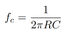
where a set of practical values might be f_c = 1Hz, C = 1 µF, R = 159kΩ. The issue with this method issue arises when we consider the current draw of the SDR - in the case of the RTL-SDR it is around 250mA. To provide this current through a (1st order) lowpass filter without causing the supply to droop significantly, we would need a huge resistor. This is problematic, since the resistor is going to get very hot, and a small resistance means our lowpass filter will have a huge cutoff frequency, so it cannot supress high frequency noise (unless we add a ridiculously large capacitor). We are in a bit of a double-bind at this point, and most designers would leave the issue alone at this point, add a ferrite bead or LC lowpass for good measure, and call it a day.
System Overview
At this point, it is clear we want to design a system with the following properties:
- Accepts an input from a convenient power source (such as a USB port).
- Strongly supresses supply noise.
- Provides sufficient output current to power an RTL-SDR.
- Does not waste lots of energy as heat, or cause the supply voltage to the SDR to droop.
Some form of linear regulator will accomplish this. Particularly, we want a low-dropout regulator (LDO), since it will consume a smaller series voltage from the supply (i.e. the voltage 'drop' is smaller). A regulator can be characterised by its ability to reject supply noise, this parameter is known as power supply rejection ratio (PSRR), and is defined as follows:

Usually, PSRR is expressed in dB. We want (ideally) an infinite PSRR, since for some unit change in the supply voltage, the output changes by zero volts (i.e. the output is an ideal voltage source). PSRR is usually frequency dependent, with PSRR degrading at high frequency (which is bad). A typical regulator might have PSRR as shown, here, for the commonly used LM317:

LM317 PSRR plot with frequency, Texas Instruments 2025
We can see that the PSRR is good at low frequency (note: 60dB corresponds to a supply noise attenuation of a million V/V, effectively, for a 1V change in the supply, the output moves by 1μV), but degrades as frequency increases. We can see at around 10kHz the PSRR begins to fall by -20dB/decade, this means that high frequency noise is not being supressed (20dB corresponds to an output change of 0.1V per 1V change on the supply, this is considered very poor).
A very high performance part from Analog Devices, the LT3045, has PSRR as shown below:

LT3045 PSRR plot with frequency, ADI 2026
We can see that this part is in a totally different league to the LM317. Note, while the LM317 provided around 10dB of PSRR @ 1MHz, the LT3045 achieves around 80dB!
One final, critical, point is about dropout voltages. The entire point of this design is to allow the RTL-SDR to get clean, regulated, power straight from the USB port. All LDOs have voltage drop across them, not as large as a linear regulator, but definitely not negligible. USB 2.0 specifies its 5V supply to ±5%, i.e. between 4.75V - 5.25V, so we know that the regulator must have a smaller dropout voltage than this in order to provide a USB 2.0 compatible output. The LT3045 has a typical dropout of 250mV at 250mA/25°C, which is small enough to fit in this range. For most well designed systems this will be more than adequate, given that the actual USB output voltage is often above ~5V. Just to be sure that the RTL-SDR will receive sufficient input voltage, I will use this LDO board with an Arduino Uno Q header board that I have designed - this board will feature a precise PoL converter that provides an output of 5.25V. This way, I can guarantee that the output voltage of the LDO board will not drop below 5V. This is the second reason that this part is particularly impressive, while other regulators require (often) a few volts of dropout voltage, the LT3045 manages to use only 250mV (typ) of dropout, while providing excellent PSRR.

LT3045 dropout voltage (typ) with output current, ADI 2026

Wider system voltage level diagram
Design
At this point, I designed a PCB in KiCad to host the LT3045. I wanted to enable USB passthrough from a host device, so that I could connect my SDR by USB to a computer (or an Arduino Uno Q as will be shown in my next blog), while having the supply get regulated by the LDO. The design is super simple, just the LDO, two, high quality 10μ X7R input and output capacitors (X7R dielectric is strongly recommended by the datasheet due to their nice properties, mainly their low ESR) and a few supporting components. The USB shields are not grounded, as this would cause horrific ground loop issues that would completely negate the use of such a nice regulator, instead they are tied to ground by a 1MΩ resistor, and a 100nF capacitor. This way they are not left floating, however if there is an ESD event (or similar transient to the USB shield) the capacitor can quickly discharge it to ground. The 5.1kΩ resistors are used to tell the USB-C host controller that this board wants 5V. The remaining resistor and capacitor are used to set the output voltage - unusually, this is done with a single resistor, not two as is more common. This is because the LT3045, as shown below, uses a current source (red) to set the voltage at the non-inverting input of the error amplifier, the user just provides the resistor (green) that this current flows in to. The voltage, then, at the non-inverting input is the output voltage (because the error amplifier is in a unity-gain configuration), and can be calculated easily from Ohm's law, for 5V we want a 50kΩ resistor. There are lots of interesting reasons that Analog Devices chose to implement the voltage reference in this way, they discuss them in the datasheet for this part (and in the application note) if you are interested.

LT3045 typical application schematic, ADI 2026
Before anyone mentions it, I did not include USB data line protection (like a TVS diode array) because I am lazy and am not planning to touch this thing once it is installed :) Below is the schematic and 3D view of the layout. The empty pads are for the USB-C and USB-A connectors (as will be shown). Most of the components are 0402's since I wanted the form factor to be as small as possible, ideally no wider than the width of the USB-A connector.

3D view of LDO board
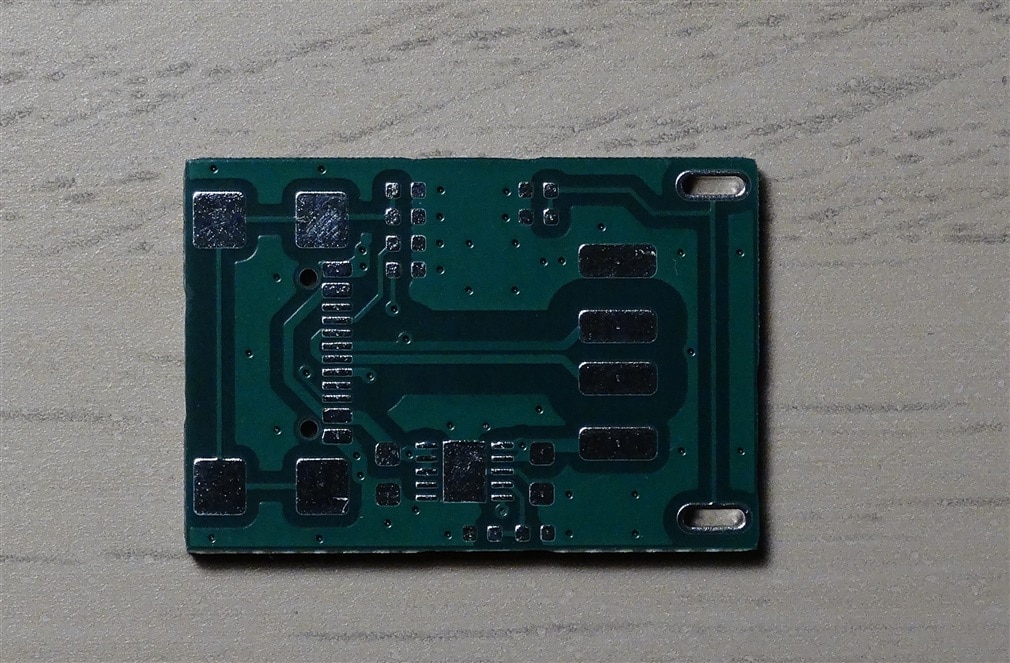
PCB

Schematic of LDO board
Bringup and Testing
Once the PCBs and parts arrived, it was just a case of soldering everything on. I used my hotplate for most of it, however I did end up re-seating the LT3045 with hot air as it didn't solder down properly due to the big thermal ground pad it has on its bottom.
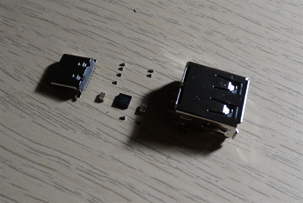
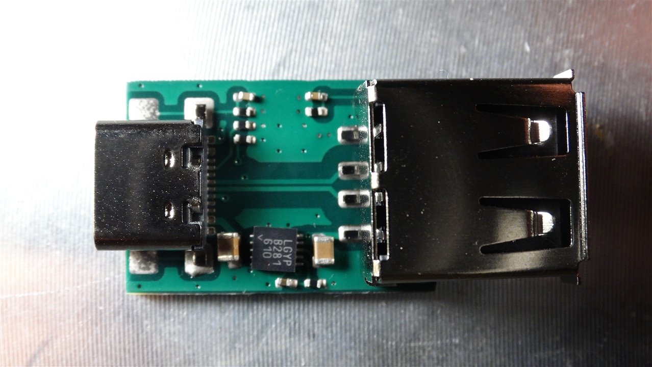
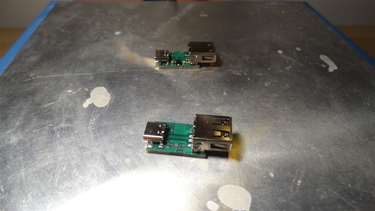
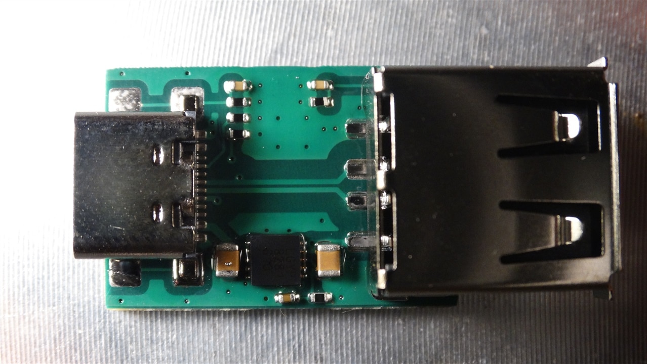
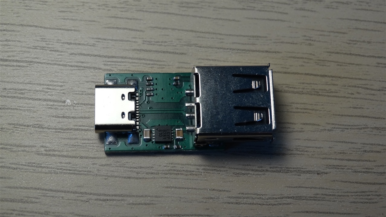
Assembly montage: Components, pre-placing components, hotplating, post-hotplate, cleaned up final board
I also made a SMA to USB-C adapter to make testing easy. The USB data lines were severed, and the supply rails were connected the the centre (Vdd) and shield (Vss) of the SMA connector respectively. This way I could easily provide a voltage to the device without using any fly-wires. It's a bit cursed but will do the job nicely.
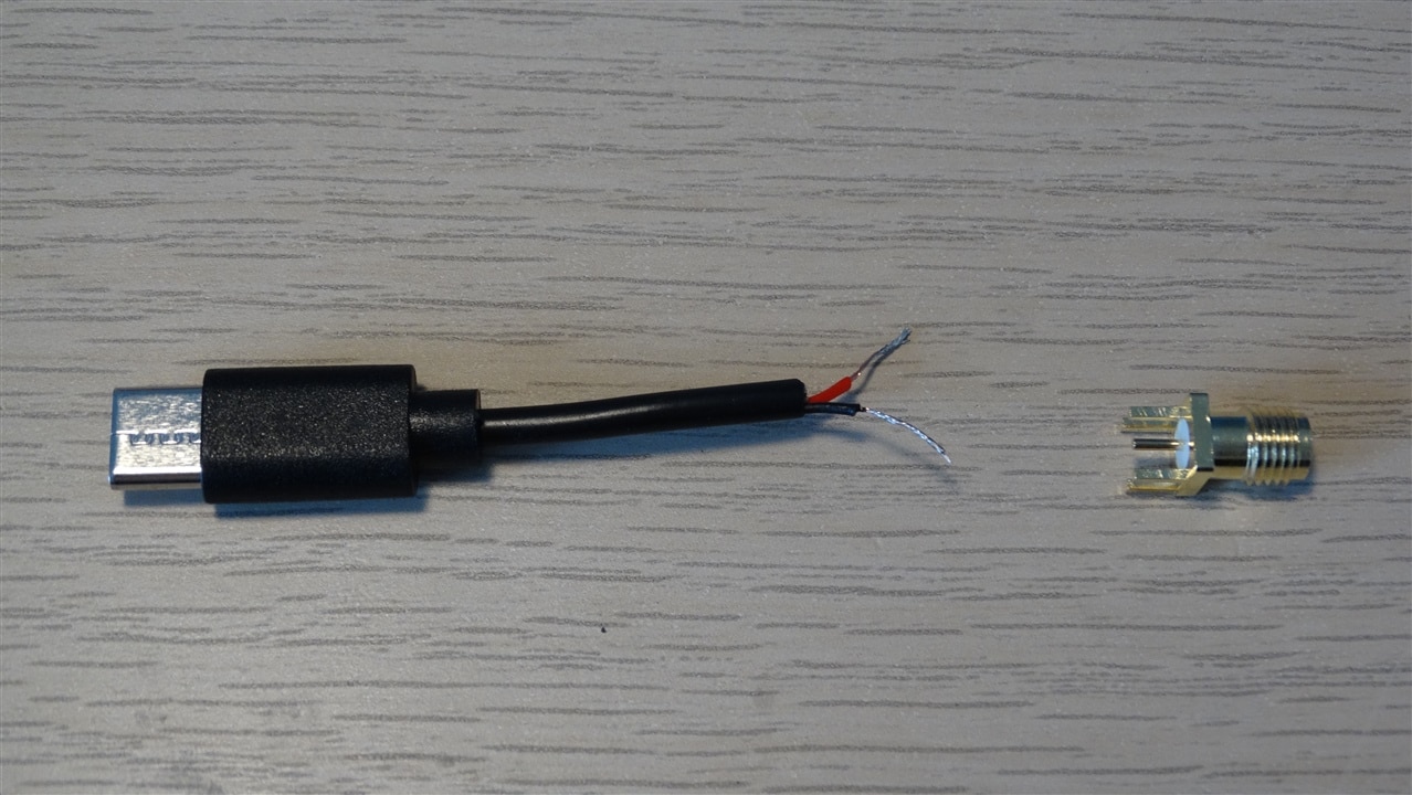
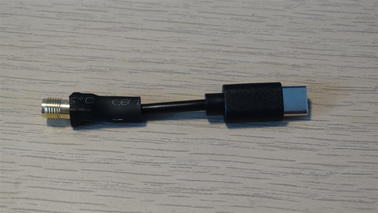
USB-C splice and SMA connector (unsoldered, soldered)
A simple DC test confirms that the output is being correctly regulated to 5V.
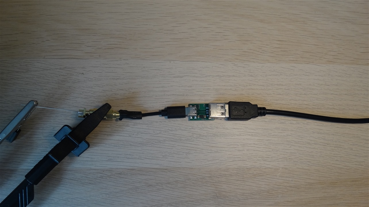
DC test setup. 6V is applied to the input through the SMA adapter (centre 6V, the shield is ground), and the output at the USB A port is measured. The exact output value is approximately 5.06V. The inaccuracy is due to me not using a precision resistor to set the output voltage
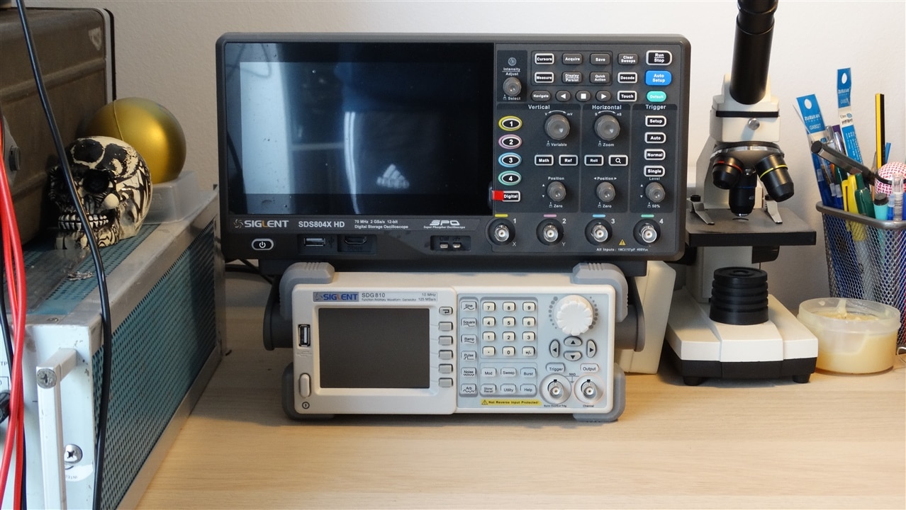
Scope and function generator, DC supplies can be seen on the left
Further to this, I wanted to obtain AC characteristics for my LDO board. My scope and function generator pair have the functionality required to measure transfer functions, in this way I could obtain the PSRR of my entire breakout board. There are many reasons that this may differ from the plot shown in the data sheet, however, any performance degradation would likely be down to bad layout. The application note for the LT3045 contains many suggested layout techniques, and I followed these to the best of my ability given the tight form factor.
Usually, to perform PSRR measurements, an AC stimulus is applied to the supply rail, and the resulting AC at the output of the LDO is measured. From the formula for PSRR, we can now calculate, given these two measurements, the PSRR (at a given frequency). Typically, to obtain the plots shown earlier, the frequency is swept to accumulate results for PSRR over a given range of frequencies. In order to apply this AC stimulus to the supply rail, we can use a bench power supply to create a reference DC voltage (in our case, this is the supply voltage we want, i.e. 5.25VDC), and an AC voltage source (for example, a sinusoid of amplitude 100mVpp generated by a function generator) which we will add to the DC reference. The two signals will be added in a high pass filter with a low break frequency (in this case, 1.6Hz). This will then be buffered (to deliver the required current), fed into the LDO board, and the output AC is measured and plotted. Ideally, the voltage references should have low noise.
A simple buffer was created using an ADA4891 high speed opamp, and a generic BC337 npn transistor. The opamp was selected since it had a large bandwidth (220MHz) and a large open loop gain. The high bandwidth product is critical, as our sweep will be performed from 10Hz-10MHz, so we need the opamp to have a much larger bandwidth than the maximum frequency in the sweep. These were connected in a common-collector configuration, with a 10Ω base resistor connecting the opamp output and transistor base.

PSRR measurement buffer circuit schematic
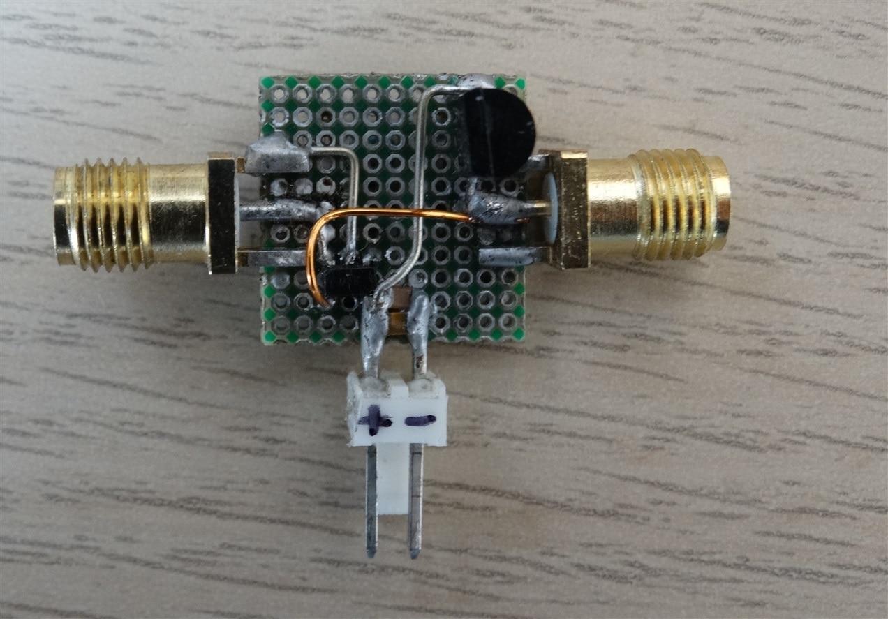
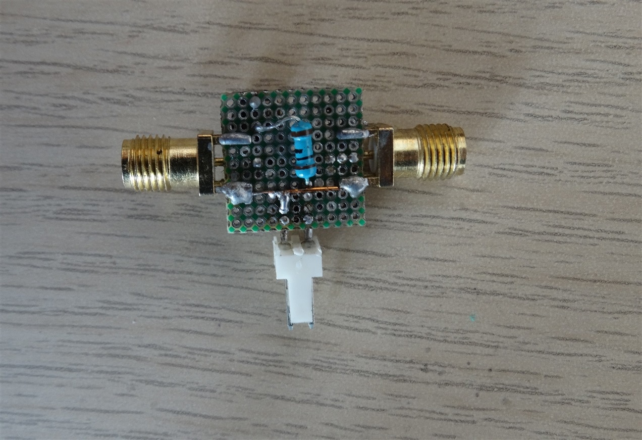
PSRR measurement buffer circuit (top, bottom)
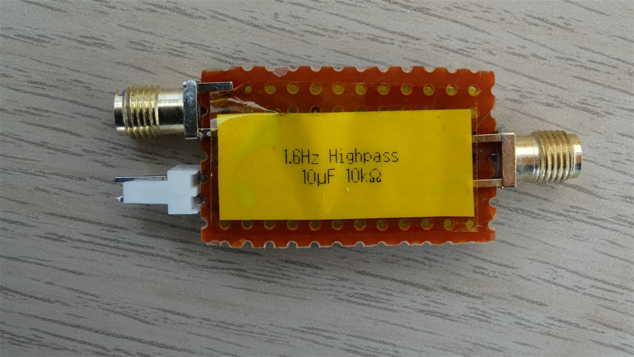
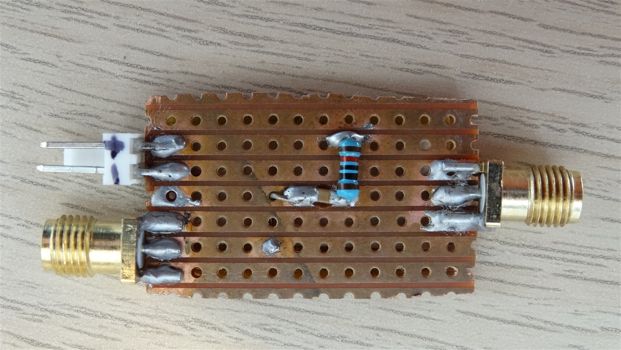
PSRR measurement high pass filter (top, bottom)
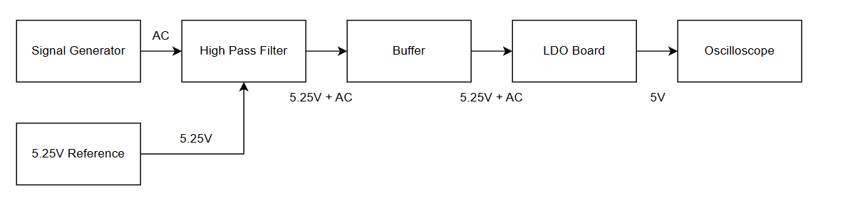
PSRR measurement methodology
Since this is getting a bit long, in my next blog I will show the full transfer characteristics of the LDO board and my measurement setup, and the impact it has on the noise floor of the SDR. Hopefully you guys found these measurement/PSRR circuits interesting, and let me know if there is anything that needs clarifying in the comments :)
Also all of this stuff is available on my git if you would like to check it out :D
-

DAB
-
Cancel
-
Vote Up
0
Vote Down
-
-
Sign in to reply
-
More
-
Cancel
Comment-

DAB
-
Cancel
-
Vote Up
0
Vote Down
-
-
Sign in to reply
-
More
-
Cancel
Children