I recently started a discussion in the "Ask an Expert" forum that described the process I used to start up an untested circuit and asked what tips other element14 members have on the subject. There were many good suggestions in the comments section and the discussion expanded. This blog will summarize my thoughts and what I learned from others in a more organized fashion. It focuses on untested PCBs and the design considerations to be made before sending a PCB off for fabrication.
Early Testing, Simulation, and Research: Testing circuits with breadboard and perfboard are good ways to gain confidence in a new design and work out some bugs. The parts used this way can be scavenged when the PCB prototype arrives if needed. Other useful techniques include simulation, a review of the manufacturer's datasheet, and study of open hardware designs in books and on the internet.
Schematic: Considerations for powering up a PCB prototype and provisions for debugging need to be made during the design stage and included in the schematic. It is good practice to break the schematic into sub-circuits with provision for sequential testing or isolation and debugging. As an illustration, the following schematic has been subdivided and will be used in the start-up and test plan that follows below.
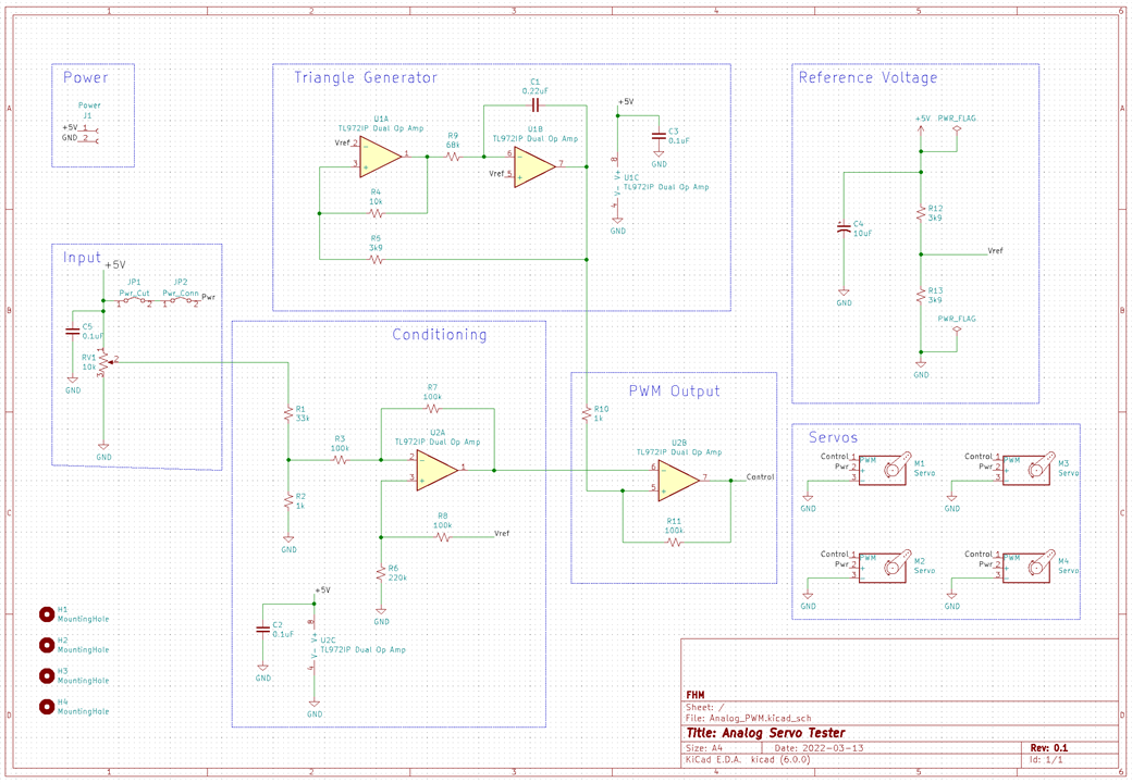
Missing from this schematic are test points. That may not be a large issue on this design since it uses through-hole components which are easily probed but on many boards that is not the case.
Test Points: Test points are invaluable for probing power, key analog signals, and buses such as SPI and I2C. Some common ways of probing single points are shown below.
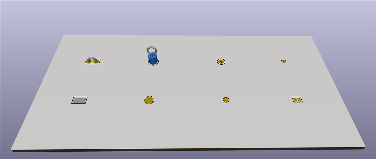
The two loop style components shown in the upper left are convenient for hands-free connection of oscilloscope probes or use with mini-grabbers. Simple through-hole pads to the right can be probed directly with a pointed probe or a pin/section of wire can be soldered in for use with grabbers. The surface mount pads lower left can be probed with a sharp probe or a bit of wire soldered on and grabbed. The last pad is a special type that can be used as an open jumper, or a solder blob can be used to short across it. There are also test points for use with an oscilloscope probe tip with spring ground tips.
Multiple points can be brought out on connectors such as the Molex Picoblade series. A 10 pin connector can make 2 grounds on either end plus 8 signals in between available to a logic analyzer.
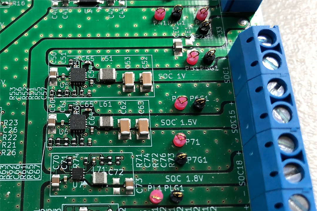
The image below shows loop-style test points on the Rohm FEFRPT001-EVK-001 power evaluation board. Note that a ground point is provided by each test point for ease of measurement.
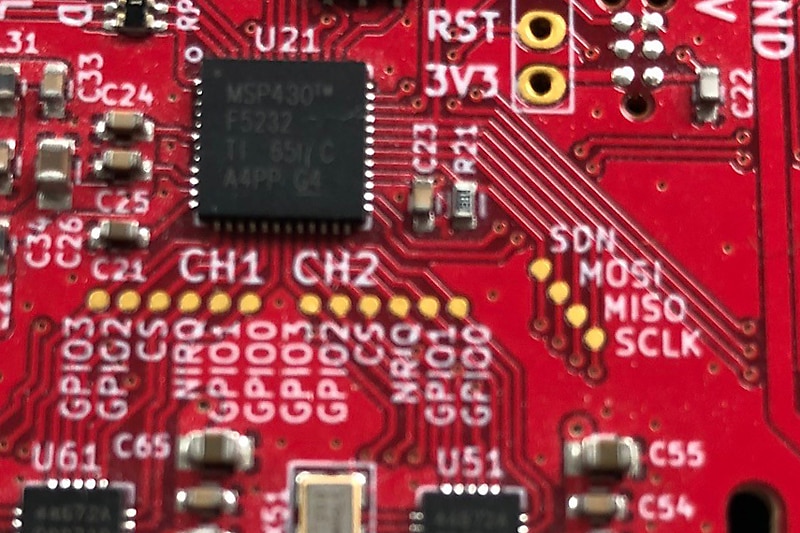
Test points can be quite small and unobtrusive as shown by the surface mount pads on the "dAISy" PCB by Wegmatt LLC shown below. Note the clear labels. The pins on this microcontroller are much easier to probe with the provided test points and markings.
Jumpers: Jumpers can be used to provide test points, a way to isolate or connect, and for other uses as illustrated by the image below. Similar surface mount arrangements are also possible.
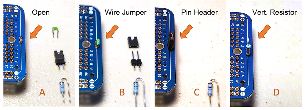
Image A shows the connection open with various connections alongside (wire, pin header with jumper, and resistor). In B, an insulated section of wire has been jumpered across to connect the two traces. If an uninsulated wire is used it could be used as a loop-style test point. C shows a pin header joining the two traces with the jumper connection in place. This allows the connection to be made or disconnected quickly. It would also be possible to measure current with a multimeter by removing the jumper and connecting between the pins. Finally, D has a 47-ohm resistor in place. A 33-ohm resistor is often used in 3V3 digital lines. Resistors can be used to limit current for protection with 100-ohm able to limit current to 33 mA with 3V3 logic.
Other Considerations: A polyfuse is good protection for more expensive boards/components. A range of current values in size 1206 are available. Ferrite beads can be used to isolate power sections and can reduce noise without undue voltage drop. An 0805 size 600-Ohm @ 100 MHz ferrite is a typical value. It is best to work with 0603 or larger parts when possible on prototypes - they are much easier to fix or connect bodge wires to with hand soldering.
Powering Up: Implementing the ideas above should make powering up and debugging easier. A bench power supply with over-voltage and current settings are advisable when possible. The following steps are commonly taken when powering:
- Start by building and testing the power supplies.
- Check that all IC power pins are properly connected to the appropriate supplies.
- Check that no outputs are shorted to rails or other outputs.
- Re-check that no connectors have been reversed.
- Assemble sub-circuits sequentially and test by section or complete assembly and test sections with isolation.
- Apply power slowly using severely restricted current from the power supply and see if anything gets hot.
- If everything works OK, check that signals are doing what they should.
For a recent project, I created a test plan where the sub-circuits were assembled sequentially and then tested before moving on. This can be simple or complex depending on the circumstances. Mine was made with a spreadsheet.
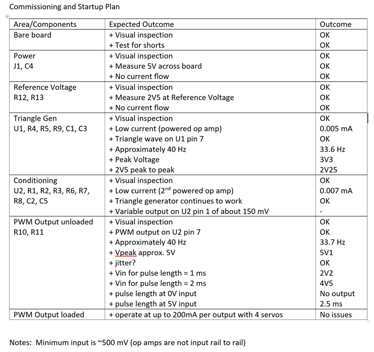
Each area / sub-circuit was broken out and the components were listed in the first column. The central column contains the steps to be taken when the sub-circuit is activated and what the expected outcome is. The final column lists the outcome. This plan could be improved by providing more detail about the steps and including maximum voltage and current settings for the bench power supply. Visual inspection of solder joints, testing for shorts, and assuring connections are not reversed should be done at every step.
Debugging: If the features above were implemented and the powering up proceeded in steps then isolating bugs to sub-circuits and the likelihood of having test points to resolve them will be greatly heightened.
If there just wasn't any room for test points, then the following can be tried with pins on ICs having in-built protection diodes. Set a DMM to diode forward voltage mode and place the positive test probe on the IO pin and the negative test lead on a respective Vcc pin. It should show ~300mV if the IO pin and at least one power pin are soldered correctly. Similarly, a test can be done with the positive lead on GND and the negative lead on the IO pin. Even correctly soldered BGA balls under the chip can be tested like that. This is best done immediately after soldering an IC to minimize false results measured from more than one component connected to a specific trace (pull-up/downs or an IC pin at the other end of the trace). An open solder joint would show no forward voltage and measuring a second IO pin would rule out the Vcc or GND pin not being soldered.
Another method that gives full access is to carefully scrape the solder mask off of the track and then solder wire wrap wire to it.
Conclusion:
Thanks to shabaz, colporteur, Andrew J, dougw, BigG, wolfgangfriedrich, Jan Cumps, jc2048 and michaelkellett for ideas, suggestions, and comments. The original comments are located here and have additional information and background.
The subject matter aligns well with the current Project14 contest on circuit prototyping but this was more of a community post so it is not intended to be eligible for prizes.
Corrections, comments, and discussions on my work are always welcome. What problem have you encountered when bringing up a new prototype that was especially difficult to solve?

Top Comments