element14 Community
element14 Community
    Register Log In
  • Site
  • Search
  • Log In Register
  • Community Hub
    Community Hub
    • What's New on element14
    • Feedback and Support
    • Benefits of Membership
    • Personal Blogs
    • Members Area
    • Achievement Levels
  • Learn
    Learn
    • Ask an Expert
    • eBooks
    • element14 presents
    • Learning Center
    • Tech Spotlight
    • STEM Academy
    • Webinars, Training and Events
    • Learning Groups
  • Technologies
    Technologies
    • 3D Printing
    • FPGA
    • Industrial Automation
    • Internet of Things
    • Power & Energy
    • Sensors
    • Technology Groups
  • Challenges & Projects
    Challenges & Projects
    • Design Challenges
    • element14 presents Projects
    • Project14
    • Arduino Projects
    • Raspberry Pi Projects
    • Project Groups
  • Products
    Products
    • Arduino
    • Avnet Boards Community
    • Dev Tools
    • Manufacturers
    • Multicomp Pro
    • Product Groups
    • Raspberry Pi
    • RoadTests & Reviews
  • About Us
  • Store
    Store
    • Visit Your Store
    • Choose another store...
      • Europe
      •  Austria (German)
      •  Belgium (Dutch, French)
      •  Bulgaria (Bulgarian)
      •  Czech Republic (Czech)
      •  Denmark (Danish)
      •  Estonia (Estonian)
      •  Finland (Finnish)
      •  France (French)
      •  Germany (German)
      •  Hungary (Hungarian)
      •  Ireland
      •  Israel
      •  Italy (Italian)
      •  Latvia (Latvian)
      •  
      •  Lithuania (Lithuanian)
      •  Netherlands (Dutch)
      •  Norway (Norwegian)
      •  Poland (Polish)
      •  Portugal (Portuguese)
      •  Romania (Romanian)
      •  Russia (Russian)
      •  Slovakia (Slovak)
      •  Slovenia (Slovenian)
      •  Spain (Spanish)
      •  Sweden (Swedish)
      •  Switzerland(German, French)
      •  Turkey (Turkish)
      •  United Kingdom
      • Asia Pacific
      •  Australia
      •  China
      •  Hong Kong
      •  India
      •  Korea (Korean)
      •  Malaysia
      •  New Zealand
      •  Philippines
      •  Singapore
      •  Taiwan
      •  Thailand (Thai)
      • Americas
      •  Brazil (Portuguese)
      •  Canada
      •  Mexico (Spanish)
      •  United States
      Can't find the country/region you're looking for? Visit our export site or find a local distributor.
  • Translate
  • Profile
  • Settings
Making Time
  • Challenges & Projects
  • Project14
  • Making Time
  • More
  • Cancel
Making Time
Blog A Crystal Clock with 1 Transistor - the Pierce Oscillator
  • Blog
  • Forum
  • Documents
  • Events
  • Polls
  • Files
  • Members
  • Mentions
  • Sub-Groups
  • Tags
  • More
  • Cancel
  • New
Join Making Time to participate - click to join for free!
  • Share
  • More
  • Cancel
Group Actions
  • Group RSS
  • More
  • Cancel
Engagement
  • Author Author: Jan Cumps
  • Date Created: 23 Nov 2020 9:27 PM Date Created
  • Views 18288 views
  • Likes 20 likes
  • Comments 35 comments
  • makingtimech
Related
Recommended

A Crystal Clock with 1 Transistor - the Pierce Oscillator

Jan Cumps
Jan Cumps
23 Nov 2020

A sweet little one-transistor crystal oscillator for the Project14 | Making Time season.

In Project14 spirit, it's only 5 ultra-cheap components.

Just off the border between analogue and digital.

image

With the 5 components we'll make a Pierce crystal oscillator. One of the most commonly used oscillators in microcontroller circuits.


The circuit is often used in digital designs, because that's where we need clocks. But in essence it's an analogue circuit.

Like every oscillation circuit, we have to have a gain > 1 at the requested frequency, when the phase is 0 or 360°. So that the circuit keeps energising itself.

This is the extremely simple schematic that does that :

image

source: National Semiconductor application note 32.


I'm going to take a lot of jumps here over the difficult stuff:

  • the JFET is an inverter, and gives us 180° of phase shift.
  • the rest has to be approximated by the rest of the circuit.

You can take this for granted, or read the document from Ramon Cerda that I provided in the sources below.

The better you approximate the 0° /  360° goal, the efficienter your oscillator.

But it's very forgiving:

  • we are already over 180° image. Before 180°, gain works against us. Once this cliff is taken, gain supports the oscillation.
  • the JFET has plenty of gain
  • the crystal is a narrow band device

So even when things are terribly off, the circuit will still want to oscillate at the crystal's frequency.

I had guaranteed success with crystals between 12 and 19 MHz. Even if the power supply ramped up slowly and there was no hard trigger event to kick off the play.

With a 4 and 4.4 MHz crystal, I had to disturb the circuit (introduce some bounce by wiggling the crystal in the socket) to get the circuit oscillating.


image


How to Build?


What components did I use:

  • a 100 µH  inductor, retrieved from a defunct VCR player Product LinkProduct Link.
  • a J112 JFET Product LinkProduct Link.
  • any 1 nF capacitor (ceramics will do just fine) Product LinkProduct Link.
  • any 10 MΩ resistor Product LinkProduct Link.
  • leftover female headers for power supply, output and to place different crystals.
  • a few crystals, from anywhere, or this very common one: Product LinkProduct Link.
  • leftover perfboard. I built it on an 8 * 6 matrix.
    Don't breadboard this circuit. It's over 10 MHz. Use perfboard or a plain copper clad PCB. Or point-to-point.
    That said, you can see in the comments that jw0752 successfully built one on a breadoard.
  • a DC supply between 3 V and 18 V. A single CR 2032 coin cell will do. Or a pair of  AA(A)s, a 9 V battery, etc. or your bench supply.


Here's the schematic I used. The same as the application note image. Just couldn't locate a 1 nF capacitor.

image


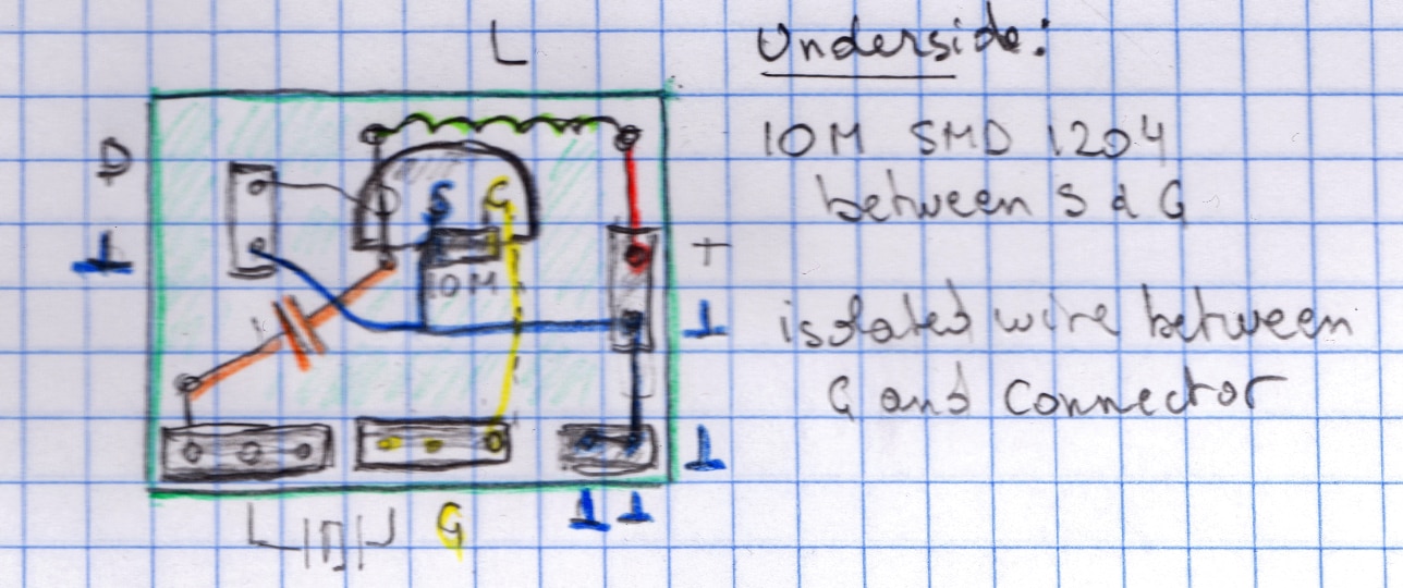
I then made a rough drawing of the perfboard layout

image


... and built it like that:

imageimage

Here is that same layout, but redrawn after all was finished.

This can help to replicate the project on some perfboard:

image

I gathered some crystals from my throwaway pile:

image

... and tested them.

image

Above with a 12 MHz crystal. Below is a scope capture with a 16 MHz crystal. Circuit powered by a 3.3 V supply:

image

Here's the Pierce crystal oscillator in action:


You don't have permission to edit metadata of this video.
Edit media
x
image
Upload Preview
image


That's the build. The remainder of the article are some further investigations in the use and operation. Feel free to skip.


The Pierce Oscillator in Practical Applications


If it is so common in microcontroller circuits, why don't I ever see the inverter or JFET on modern designs, or on LaunchPads, Arduinos, MBED boards?

That's because most microcontrollers have the inverter part of the circuit implemented internally already. You just need to provide the crystal and 2 capacitors.

Here's a Hercules ARM microcontroller datasheet's schematic of the internal parts (abstracted). In essence it's the same Pierce circuit.


image


Why do I say it's an analogue circuit, when it is often implemented with a NOT gate?

Well, you'll see that when a NOT gate is used, the designers put a resistor in parallel between the output and input of the gate.

image

source: the article William bases his design on.

That resistor, together with the gate's input impedance and the capacitor at the input, turn this gate into an analog amplifier. We're perverting its digital behaviour and turn it into a high gain transistor (like, say, a JFET image ). That's why it only works with a subset of logic NOT gates. It wouldn't work if you'd simulate one in an FPGA.

You'd expect a perfect square wave on the output, but I challenge you to build this circuit and probe the output.


It's featured in textbooks:
image

source: photo of Figure 7.38A taken from my copy of The Art of Electronics


The exact same design is featured in The Art of Electronics by Horowitz and Hill.

They use a 2.5 mH and the now as good as obsolete 2N5485 JFET.


Looking at Gate vs Output


This is a common source n-channel JFET design, where the source is tied to the ground and is shared by input and output.

Here are the gate and drain captured, relative to that source (ground) shared point

The input source is a 9 V battery.

Both signals use the same 0 position on the oscilloscope screen and the same scale.

: The ground level is where you see this in the image below.image

image


As you can see, there's a lot happening.

One of those things is, that the gate is being pushed down to 15 V negative.


Sources:

The design comes from a National Semiconductors (now TI) Application Note.

The discussion of splatkillwill was the inspiration for this post.

The excellent article of Ramon Cerda dives into the practical considerations when building reliable oscillators.

  • Sign in to reply

Top Comments

  • jw0752
    jw0752 over 4 years ago +5
    Hi Jan, I checked my inventory and I had a 2N5459 which is an N Channel JFET so I was able to build the original circuit. It is amazing what a nice simple circuit it is. Here is my bread board with a 16…
  • dubbie
    dubbie over 4 years ago +5
    Jan, You have a throw away box - that you haven't thrown away! I find that bits just disappear by themselves. I suspect they might be falling off the edge of my desk but I don't want to look.- just in…
  • Jan Cumps
    Jan Cumps over 4 years ago in reply to Jan Cumps +5
    Jan Cumps wrote: I'll try to correlate the drain current vs gate voltage this weekend. A small resistor in series shouldn't break the design. I have a few low resistors here. Not precise, but that doesn…
Parents
  • dubbie
    dubbie over 4 years ago

    Jan,


    You have a throw away box - that you haven't thrown away! I find that bits just disappear by themselves. I suspect they might be falling off the edge of my desk but I don't want to look.- just in case I find everything I've lost actually is on the floor at the back of my desk. It would be a lot of things.


    Dubbie

    • Cancel
    • Vote Up +5 Vote Down
    • Sign in to reply
    • More
    • Cancel
  • jc2048
    jc2048 over 4 years ago in reply to dubbie

    I was going to try Jan's circuit for myself, but can I find a 100uH inductor? No.

    • Cancel
    • Vote Up +3 Vote Down
    • Sign in to reply
    • More
    • Cancel
  • Jan Cumps
    Jan Cumps over 4 years ago in reply to jc2048

    The 100 µH is random. It was either that one or a 6µH.

    Without inductor, the circuit doesn't oscillate. When I shortcut it while the circuit oscillates, it stops.


    Warning when trying this at home: set a current limit on your power supply. Because when it doesn't oscillate, the FET conducts.

    I've put the current limit to 45 mA. Enough to get the circuit bootstrapped.

    If I limit the current at 41 mA or lower, it does not start up, yet consumes that high current constantly.

    From 42 mA on, it starts oscillating and the current drops to 2 mA once in steady state.

    • Cancel
    • Vote Up +3 Vote Down
    • Sign in to reply
    • More
    • Cancel
  • jc2048
    jc2048 over 4 years ago in reply to Jan Cumps

    The datasheet is vague about the Idss value, it just gives a minimum of 5mA.


    image


    The model in Tina-TI has a much higher figure [28mA], though it's still less than the 41mA you seem to be seeing.


    image

    • Cancel
    • Vote Up +1 Vote Down
    • Sign in to reply
    • More
    • Cancel
  • Jan Cumps
    Jan Cumps over 4 years ago in reply to jc2048

    jc2048  wrote:


    The datasheet is vague about the Idss value, it just gives a minimum of 5mA.

    The model in Tina-TI has a much higher figure [28mA], though it's still less than the 41mA you seem to be seeing.


    It will happily drain 5 or 28 mA straight to ground. But it doesn't oscillate below +- 41 mA.

    I'll try to correlate the drain current vs gate voltage this weekend.

    A small resistor in series shouldn't break the design. I have a few low resistors here. Not precise, but that doesn't matter to visualise the broad context.


    The speed at which it starts to oscillate is a function of the max current I allow in the circuit.

    2.8 V or 9 V Vcc doesn't make a lot of difference. But capping the max current at 42 or 70 mA makes a big change in the startup behaviour.

    • Cancel
    • Vote Up +3 Vote Down
    • Sign in to reply
    • More
    • Cancel
Comment
  • Jan Cumps
    Jan Cumps over 4 years ago in reply to jc2048

    jc2048  wrote:


    The datasheet is vague about the Idss value, it just gives a minimum of 5mA.

    The model in Tina-TI has a much higher figure [28mA], though it's still less than the 41mA you seem to be seeing.


    It will happily drain 5 or 28 mA straight to ground. But it doesn't oscillate below +- 41 mA.

    I'll try to correlate the drain current vs gate voltage this weekend.

    A small resistor in series shouldn't break the design. I have a few low resistors here. Not precise, but that doesn't matter to visualise the broad context.


    The speed at which it starts to oscillate is a function of the max current I allow in the circuit.

    2.8 V or 9 V Vcc doesn't make a lot of difference. But capping the max current at 42 or 70 mA makes a big change in the startup behaviour.

    • Cancel
    • Vote Up +3 Vote Down
    • Sign in to reply
    • More
    • Cancel
Children
  • Jan Cumps
    Jan Cumps over 4 years ago in reply to Jan Cumps

    Jan Cumps  wrote:


    I'll try to correlate the drain current vs gate voltage this weekend.

    A small resistor in series shouldn't break the design. I have a few low resistors here. Not precise, but that doesn't matter to visualise the broad context.


    Here's  capture. Without analysing.

    Yellow: the output voltage at the drain

    Blue: gate voltage

    Violet: drain current. 1 V = 1 A.


    image

    one cycle:

    image

    • Cancel
    • Vote Up +5 Vote Down
    • Sign in to reply
    • More
    • Cancel
  • jc2048
    jc2048 over 4 years ago in reply to Jan Cumps

    Without analysing.

    Nope. Me neither. I don't understand why the current is three times the frequency.


    I think you need to draw us a picture of how you're doing the current measurement.

    • Cancel
    • Vote Up +1 Vote Down
    • Sign in to reply
    • More
    • Cancel
  • Jan Cumps
    Jan Cumps over 4 years ago in reply to jc2048

    jc2048  wrote:


    I think you need to draw us a picture of how you're doing the current measurement.

    image


    I put a 1R in series with the inductor. Probed it with a 70 MHz differential probe.

    • Cancel
    • Vote Up +3 Vote Down
    • Sign in to reply
    • More
    • Cancel
  • jc2048
    jc2048 over 4 years ago in reply to Jan Cumps

    Nice picture.


    You've just added some Cs from the differential probe tips. Do you have long leads from the PSU? If so, that's some additional small inductance, so maybe it's an interaction between all those.


    Perhaps try, either some decoupling across the rails at the board [maybe 10uF electrolytic + 100n ceramic] and see if it goes away, or vary the differential probe tip Cs by adding say
    additional 10pF caps and see if the higher frequency you see comes down in frequency.


    It's possible, I suppose, that you have the crystal running in the fundamental mode and the 3rd overtone mode at the same time, aided by the now quite complicated load.


    Another approach would be to put the current measuring resistor in the ground connection so that it and the differential probe don't complicate the load seen by the FET.

    • Cancel
    • Vote Up +1 Vote Down
    • Sign in to reply
    • More
    • Cancel
  • Jan Cumps
    Jan Cumps over 4 years ago in reply to jc2048

    A better probe attempt of the gate and drain voltage only.

    Powered from a 9 V cell with short leads. Both oscilloscope probes with pigtail ground leads.


    image


    image


    I removed the current shunt. Wiring it up between source and ground is a bit tricky with my current design.

    I have to clip the source mead of the FET for that and bodge the shunt in between that and ground.

    Because that's a cement 5 W power resistor, it's a bit involved. I prefer to do that with daylight available.

    • Cancel
    • Vote Up +3 Vote Down
    • Sign in to reply
    • More
    • Cancel
element14 Community

element14 is the first online community specifically for engineers. Connect with your peers and get expert answers to your questions.

  • Members
  • Learn
  • Technologies
  • Challenges & Projects
  • Products
  • Store
  • About Us
  • Feedback & Support
  • FAQs
  • Terms of Use
  • Privacy Policy
  • Legal and Copyright Notices
  • Sitemap
  • Cookies

An Avnet Company © 2025 Premier Farnell Limited. All Rights Reserved.

Premier Farnell Ltd, registered in England and Wales (no 00876412), registered office: Farnell House, Forge Lane, Leeds LS12 2NE.

ICP 备案号 10220084.

Follow element14

  • X
  • Facebook
  • linkedin
  • YouTube