Op-amps are evolving as they now add specialized performance functions tailored to suit specific end applications. Zero drift, precision performance, and higher voltage rails are some of the specialty functions that are gaining ground today. Let’s put these developments into context. Traditional op-amps experienced the problem of drift due to temperature and aging over time. A new class of zero drift amplifiers addresses this problem by dynamically correcting the offset voltage and providing the precision performance with an internal solution. The problem with traditional 5V op-amps is that they need complex external circuitry to make the input signals compatible for signal conditioning, and the outputs also need to be conditioned to connect to heavy loads. In contrast, high voltage op-amps are now loaded with features such as overvoltage protection, EMI filtering, MUX compatibility, and high current feedback, which help to simplify the external circuitry. This module will cover the unique features, functions, and circuits incorporated in specialty op-amps dedicated for high voltage and precision applications.
Related Components | Test Your Knowledge
2. Objectives
Upon completion of this learning module, you will be able to:
- Describe the architecture of high voltage op-amps and discuss their characteristics
- Understand the specialized functions required for high voltage op-amp designs
- Explain the implementation of high voltage op-amps in precision applications
3. Review
We discussed the operation, connection, configurations, and characteristics of op-amps in the first module of this series. Please visit the first learning module if you would like to review that discussion.
4. Characteristics of High Voltage Op-amps
A high voltage operational amplifier in simple terms is nothing but a general purpose operational amplifier with the capacity to handle high voltage and current. Some of their salient features are:
- Can operate at high voltage power rails in the range of above +/-27V
- Accept high voltage inputs
- Deliver current from 10mA all the way up to 10000mA with good linearity
- Gain bandwidth ranges from 0.55 MHz all the way up to 8GHz
- High open-loop gain in the range above 100 dB
- Have a high gain-bandwidth product (GBWP) with extremely high slew rates greater than 200V/µs
- Have a wide common mode range and high DC precision as low as 5 µV
- Extremely low input bias current
- Very low noise in the range of 5nV/√Hz
- High voltage transient protection at the inputs
5. Design of High Voltage Op-amps
One way to allow a general purpose op-amp to operate at high voltage and current is to replace the standard components inside it with high voltage discrete components such as MOSFETs. This would typically result in a three-stage amplifier. The first stage is a differential amplifier which converts the differential voltage to a current output. The second stage operates in common emitter configuration and gives an amplified voltage from the current input. The final output stage consists of a pre-amplifier and output transistor and works as a unity gain voltage amplifier with increased current.
Another way would be to modify internally a general purpose op amp to incorporate a power booster circuit. The booster stage is placed between the feedback pins of the op amp to maintain the stability and gain characteristics of the amplifier.
- 5.1 Trimming and Offset Correction Methods
Amplifier input offset voltage is often the key parameter for design accuracy, and there are different circuit techniques used to minimize it. Knowing the various trimming and offset correction methods may be productive when selecting an amplifier for a particular application.
One method is laser trimming, which is performed on the die at the time of manufacturing by trimming the internal resistor to achieve a nulled offset voltage. However, stresses at the time of device packaging may produce shifts in the offset voltage.
Another method used to achieve low offset voltage and drift is e-Trim, which is Texas Instruments’ patented trimming architecture implemented after device packaging. Correction current sources internal to the devices are adjusted during the final package-level manufacturing test. Once the trimming is completed, the gateway to trim circuitry is closed, so the trim control circuit is disabled and the adjustments become permanent. This polysilicon, fuse-blowing technique does not require extra pins or test pads and provides substantial improved performance over wafer-level trim. This approach also avoids the parameter shifts that typically occur as a result of package stress, producing the excellent precision only possible with zero-drift amplifiers and allowing miniature package sizes.
The final method is the chopper amplifier. Although it is not a trim method, chopper amplifiers are used to correct offset and drift. The chopper is a common type of zero-drift amplifier that uses an internal dynamic calibration method to minimize the offset voltage.
6. Specialty Functions in Precision and High Voltage Op-amps
High voltage and precision op-amp circuits need features such as zero drift, ultra-low noise, MUX friendliness, high current feedback, and very low offset voltages based on the end applications. In high voltage data acquisition systems, it is necessary to convert high-voltage signals to levels acceptable to low-voltage data converters with differential inputs. This requires additional circuit configurations, like differential pair inputs and zero drift architectures, to be integrated into op-amps to enable easy and reliable implementation. We will discuss a few such circuits and architectures in this section.
- 6.1 High Voltage Op-amps in Zero-drift amplifier applications
Zero-drift amplifiers employ a unique, self-correcting technology which provides ultra-low input offset voltage (VOS) and near-zero input offset voltage drift over time and temperature (dVOS/dT) suitable for general and precision applications. TI’s zero-drift topology also delivers other advantages, including no 1/f noise, low broadband noise, and low distortion – simplifying development complexity and reducing cost. This may be done two ways: using a chopper amplifier or via autozeroing.
Zero-drift amplifiers are suitable for a wide variety of general-purpose and precision applications that benefit from stability in the signal path. The excellent offset and drift performance of these amplifiers make them especially useful early in the signal path, where high gain configurations and interfacing with micro-volt signals are common. Applications that benefit from this technology include precision strain gauge and weight scales, current shunt measurement, thermocouple-, thermopile-, and bridge-sensor interfaces.
Chopping zero-drift amplifiers' internal structure can have as many stages as continuous-time amplifiers. The main difference is that the input and output of the first stage has a set of switches which inverts the input signal every calibration cycle. Figure 1a shows the first half cycle. In the first half cycle, both sets of switches are configured to flip the input signal twice, but the offset flips once. This keeps the input signal in phase but the offset error polarity is reversed.

Figure 1a: First Half Cycle

Figure 1b: Second Half Cycle
Figure 1b shows the second half cycle. Here, both sets of switches are configured to pass the signal and offset error through unaltered. Effectively, the input signal is never out of phase, remaining unchanged from end to end. Since the offset error from the first clock phase and second clock phase are opposite in polarity, the error is averaged to zero.
- 6.2 High Voltage Op-amps in Multiplexing Applications
A multiplexer (MUX) works as a switch in a data acquisition system to connect a selected channel of input to a single data converter. A precision amplifier is placed after a multiplexer to drive the analog to digital converter precisely and to ensure accurate processing. Since the output of the op-amp does not change rapidly, a large voltage appears at the input of the op-amp. To respond to this condition, anti-parallel diodes are added to protect against a sharp increase in the input bias current. Refer to Figure 2a.
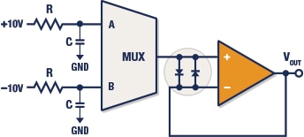
Figure 2a: MUX with Buffer-Configured Op Amp
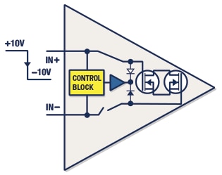
Figure 2b: MUX-friendly Scheme (High to Low Input Step)
But the anti-parallel diodes are not required in a new 36-V CMOS input circuitry design by Texas Instruments. These MUX-friendly amplifiers are still able to maintain the same level of protection and robustness while also improving settling time for switched systems. This patented input protection scheme uses a set of internal switches which open and close to protect the input of the op amp when large voltage steps are applied. This protection scheme has the added benefit of no inrush current. When the positive input goes low (+10 V to –10 V), the control block opens the switch at the inverting terminal (IN-) and activates one of the diodes. When the positive input goes high (–10 V to 10 V), the control block opens the switch at the noninverting terminal (IN+) and activates the other diode. Refer to Figure 2b.
OPA189 and OPA2189 are examples of MUX-Friendly precision high voltage op-amps used in the application of high-resolution ADC driver amplifiers, high voltage multiplexed data-acquisition systems, high precision comparators, and test and measurement equipment.
The TMUX6104 is a complementary metaloxide semiconductor (CMOS) analog multiplexer for use in high precision measurement applications. It has very low on and off leakage currents and ultra-low charge injection. It also provides excellent isolation capability by blocking signal levels up to the supplies when the switches are in the OFF position. A low supply current of 17 μA enables usage in portable applications.
- 6.3 Fully Differential Amplifier
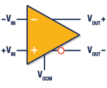
Figure 3: Fully Differential Amplifier
We can define a fully differential amplifier (FDA) as a flexible device which generates a purely differential output signal focused on a user-configurable common-mode voltage usually matched to the input common-mode voltage required by an ADC. It is similar in architecture to a standard voltage feedback operational amplifier. Both types of amplifiers have differential inputs, but fully differential amplifiers have differential outputs, as opposed to a standard operational amplifier, which has a single-ended output.
In a fully-differential amplifier, the output is differential, and the output common-mode voltage can be controlled independently of the differential voltage. The purpose of the Vocm input is to set the output common-mode voltage. See Figure 3. In a standard operational amplifier with single-ended output, the output common-mode voltage and the signal are the same thing. There is typically one feedback path from the output to the negative input in a standard operational amplifier. A fully-differential amplifier has multiple feedback paths.
When signals are transmitted from one place to another, noise is coupled into the wiring. In a differential system, keeping the transport wires as close as possible to one another makes the noise coupled into the conductors appear as a common-mode voltage. Noise that is common to the power supplies also appears as a common-mode voltage. Since the differential amplifier rejects common-mode voltages, the system is more immune to external noise.
The THS4551 is an example of a precision fully differential amplifier which offers an easy interface from single-ended sources to the differential output required by high-precision analog-to-digital converters (ADCs). It is designed for exceptional dc accuracy, low noise, and robust capacitive load driving; this device is well suited for data acquisition systems where high precision is required, along with the best signal-to-noise ratio (SNR) and spurious-free dynamic range (SFDR) through the amplifier and ADC combination. Refer to the Related Components page to learn more.
- 6.4 Current Feedback Amplifier
A current feedback operational amplifier (CFA) is a type of amplifier circuit which has an inverting input that’s more sensitive to current. They find applications in high voltage arbitrary waveform generators, power FET drivers, high capacitance piezo drivers, and VDSL line drivers.
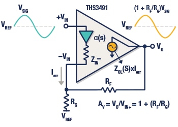
Figure 4: Functional Block Diagram (THS3491)
An example of a high voltage current feedback amplifier is the THS3491 in Figure 4. It operates at 900 MHz and offers excellent performance for applications demanding low distortion at high output power from DC through values higher than 100 MHz at 100-Ω loads. Over a wide range of gain, this current feedback design holds near constant bandwidth and distortion. This IC gives 8000 V/µs of slew rate which delivers a 10 VPP output to drive the demanding loads.
7. Applications for High Voltage Precision Systems
In this section, we will focus on some interesting applications where high voltage op-amps are utilized.
- 7.1 High Voltage Op-amps in Attenuator Amplifier Applications
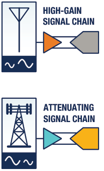
Figure 5: High Gain versus Attenuating Signal Chains
Data-acquisition systems and digitizer front-ends are often paired with high-sensitivity sensors that produce low-level output signals (i.e., measuring the voltage drop across a low-resistance shunt to measure the current in the circuit). In such cases, the amplifier signal chains are configured in high gains to maximize the dynamic range of the ADC. High-precision, differential input ADCs are typically limited to a maximum recommended supply of 5 V and a corresponding maximum differential input range of 10 VPP when the reference voltage (VREF) is set to 5 V.
However, in high-power industrial signal chains, the input signal to the system can be much larger, in which case the amplifier signal chain must attenuate the signal input down to the acceptable input range of the ADC. Figure 5 shows a simple illustration of the difference between a low signal input and high signal input ADC front end.
To design a system for this type of signal chain, some important factors such as bandwidth, slew rate, distortion, and power should be considered. For example, a high power industrial data acquisition system that requires high input impedance, low input bias current, and a rail-to-rail input and output can be designed with a high voltage op-amp such as the OPA2810. It is a dual-channel, FET-input, voltage feedback operational amplifier with low input bias current, a high supply range of 27V, and high gain bandwidth product of 70 MHz. It’s commonly used in a buffer configuration in front of the differential amplifier. The OPA2810 is unity-gain stable with a small-signal unity-gain bandwidth of 105 MHz, and offers excellent DC precision and dynamic AC performance at a low quiescent current (IQ) of 3.6 mA per channel (typical). Figure 6 illustrates the high input impedance signal chain using the OPA2810.
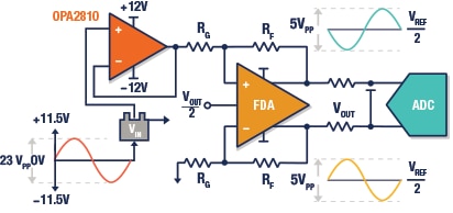
Figure 6: High Impedance Signal Chain with High Voltage Op Amp Buffer Stage
For this type of signal chain, Table 1 shows the attenuation needed in the FDA stage based on the input signal and the 5-V maximum allowed ADC input, and the common-mode input swing the FDA must support. VREF is assumed to be 5 V and hence VOCM is set at 2.5 V.
| HIGH-Z BUFFER | INPUT SIGNAL SWING | ATTENTUATION (RF/RG) | VIN_CM | VIN_CM SWING |
| OPA2810 | -11.5V to +11.5V | 5V / 11.5V to 0.44V | 1.96VDC ± 1.74V | 0.22 to 3.7V |
Table 1: Attenuation Needed in FDA Buffer Stage
- 7.2 Wideband Transimpedance Amplifier
JFET-input amplifiers are used in photodiode transimpedance amplifiers. In wideband photodiode transimpedance applications, the photodiode current is converted into a voltage using an amplifier. Although a high-speed amplifier’s gain-bandwidth product is useful for achieving a large closed-loop gain, the low input current noise and bias currents in a JFET-input amplifier help improve output noise performance in circuits using high to very high transimpedance gains, while also reducing output voltage offsets due to bias currents.
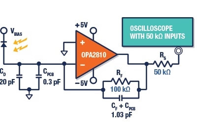
Figure 7: Wideband, High Sensitivity, Transimpedance Amplifier
In this example, we show the advantages of using JFET-input amplifiers with the OPA2810. The OPA2810 is a 110MHz, 27V, wide-input differential voltage (VIN,Diff) tolerant rail-to-rail input/output FET input amplifier. This design can support a bandwidth higher than 2 MHz and provides transimpedance gain of 100Kohms and a photodiode capacitance of 20pF. The low input noise of the OPA2810, the GBP of 70 MHz, and the low-frequency output noise of 0.45nV/√kHz make it suitable for the design. See Figure 7.
- 7.3 Multichannel-input data-acquisition systems
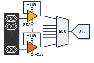
Figure 8a: A multichannel sensor front end connected to the inputs of a multiplexer
High-impedance input amplifiers are particularly useful when interfaced with sensors that have relatively high output impedance. Such multichannel systems usually interface these sensors with the signal chain through multiplexers. Figure 8a shows a circuit with an amplifier to interface with each sensor and connected to the inputs of a multiplexer.
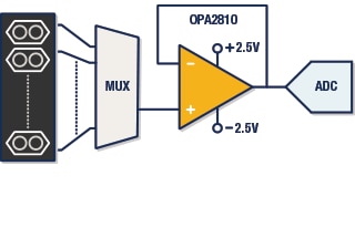
Figure 8b: A multichannel sensor front end with a single fast-settling amplifier at the output of a multiplexer that is directly connected to the sensors
An alternative would be to use a single fast-settling amplifier at the output of a multiplexer that is directly connected to the sensors. This gives rise to large signal transients when switching between channels, where the amplifier’s settling performance and maximum allowed input differential voltage begin to matter. See Figure 8b.
Figure 9 shows the output voltage and input differential voltage when applying an 8V step at the noninverting input of the OPA2810 configured as a unity-gain buffer.
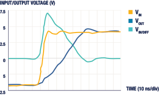
Figure 9: Large-signal transient response using a fast settling amplifier
Because of the fast input transient, the amplifier is slew-limited and the inputs cease to track each other (a maximum VIN,Diff of 7V is seen Figure 9) until the output reaches its final value and the negative feedback loop is closed. For standard amplifiers with a 0.7-1.5V VIN,Diff rating, you must use current-limiting resistors in series with the input pins to protect from irreversible damage, which also limits the device frequency response. The OPA2810 has in-built input clamps that allow the application of as much as 7V of VIN,Diff, with no need for external resistors and no damage to the device or a shift in performance specifications. Such an input-stage architecture, coupled with its fast settling performance, makes the OPA2810 a good fit for multichannel sensor multiplexed systems.
- 7.4 Differential Load Cell or Strain Gauge Sensor Signal Conditioning
In this application, two OPAx189 devices are used as instrumentation amplifiers and connected with strain gauge sensors along with the ADC for signal conditioning of a load cell or strain gauge. In Figure 10, a pair of OPAx189 amplifiers are configured in a two-amp instrumentation amplifier (IA) configuration and are band-limited to reduce noise and allow heavy capacitive drive. The load cell is powered by an excitation voltage (denoted VEX) of 5V and provides a differential voltage proportional to force applied. The differential voltage can be quite small, and both outputs are biased to VEX / 2.
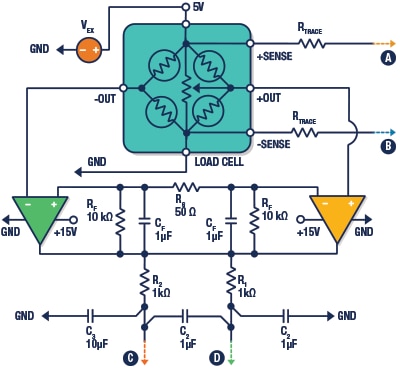
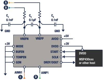
Figure 10: 24-Bit, Delta-Sigma, Differential Load Cell or Strain Gauge Sensor Signal Conditioning
In this case, the very low input offset voltage (0.4 µV), input offset voltage drift (0.005 µV/°C), the low broadband noise (5.2 nV/√Hz) and features like zero-flicker noise, excellent linearity, and the high input impedance of the device make it a solution for providing accurate signal conditioning. The two-amp IA configuration removes the dc bias and amplifies the differential signal of interest and drives the 24-bit, delta-sigma ADS1225 analog-to-digital converter (ADC) for acquisition and conversion.
*Trademark. Texas Instruments is a trademark of Texas Instruments Inc. Other logos, product and/or company names may be trademarks of their respective owners.
Shop our wide range of high voltage, precision, instrumentation, isolation, differentials op amps and more.
Test Your Knowledge
Op Amps II
Are you ready to demonstrate your Essentials of Specialty Op-amps for High Voltage and Precision Applications knowledge? Then take a quick 15-question, multiple-choice quiz to see how much you've learned from this module.
To earn the Op Amps II Badge, read through the module, attain 100% in the quiz at the bottom, and leave us some feedback in the comments section.


Top Comments