A programmable system-on-chip (SoC) can be found in many applications, such as IoT or Industry 4.0, due to its unique capabilities of being both hardware and software programmable. This module will help anyone interested in getting started with Programmable SoCs by providing an introduction to programmable SoCs, their architecture and development, their surrounding developed ecosystems, and how to overcome common barriers.
Related Dev Boards | Test Your Knowledge
2. Objectives
Upon completion of this module, you will be able to:
- Explain the differences between various types of SoCs
- Describe the structure of a programmable SoC
- Understand the difference between symmetric and asymmetric multiprocessing
- Discuss the programmable SoC development cycle
3. What is an SoC?
A system-on-chip can describe several different types of devices. At a conceptual level, it describes a device that can implement system functionality without the need for other devices. For example, an SoC may contain:
- Processing capability using either a central processing unit (CPU) or a microprocessor (MCU)
- Interfacing (e.g. SPI, UART, I2C, Giga Bit Ethernet or PCIe)
- Volatile and Non-Volatile Memory
- Analog / Mixed signal converters
- RF functionality
- Graphics Processing Unit (GPU)
While we may think of SoCs as being complicated devices, they actually cover a range of complexities and capabilities. This enables engineers to pick the most appropriate SoC for their application. One example of an SoC that many developers will be familiar with is the Broadcom SoC used on the Raspberry Pi.
To increase the processing capacity available, many SoCs contain several processing elements, implementing dual, quad, or octal core processors. The configuration of the multiple processor cores provides one of the first SoC classification methods.
When processors within an SoC are all identical, and use the same instruction set, the SoC is classified as a homogeneous SoC. If the processors are from different families or have different instruction sets, the SoC is classified as a heterogeneous SoC, as each processor in the system is different.
The choice of implementing a solution based upon a homogeneous or heterogeneous SoC depends upon the end application. Homogeneous SoCs are very useful when a high-level operating system (e.g., Embedded Linux) is deployed and the operating system load-balances across the available processor cores. A heterogeneous SoC may be selected when the different processor cores are used for different functions (e.g., application processing and real-time control).
The class of heterogeneous SoCs also includes those SoCs which include not only different types of processors, but also include programmable logic. These devices are more commonly called programmable SoCs to reflect the inclusion of programmable logic.
4. What is a Programmable SoC?
While classified as heterogeneous vs. homogenous SoCs, programmable SoCs can be further classified as either a hard programmable SoC or a soft programmable SoC.
A hard programmable SoC will implement the processor elements directly within the silicon of the device. A typical example of a hard programmable SoC is the Xilinx Zynq-7000 series of devices, which combine Arm A9 processors with programmable logic. Commonly used processors in hard programmable SoC applications are based upon Arm, Intel, and Power PC architectures. Of the two classes of SoCs, hard SoCs offer the highest performance.
A soft programmable SoC, on the other hand, does not implement the processor directly within the silicon; rather, the processor is implemented within the programmable logic of an FPGA. This provides for flexibility in the creation of the processor solution, but typically a soft SoC offers a lower performance than a hard programmable SoC. Softcore processors can be either proprietary, as is the case with the MicroBlaze and NIOS softcore processors, or open source, such as the RISC-V.
While it could be argued that a soft programmable SoC is just an FPGA design, the implementation of a processor soft core and the associated system interfaces required for the application do meet the definition of a system-on-chip.
5. Why Use a Programmable SoC?
Whichever type of programmable SoC you choose to use, they both offer a significant advantage over the traditional SoCs that do not contain programmable logic.
While traditional SoCs contain standard interfaces (e.g. SPI, I2C, GigE, and PCIe), the number of each type is limited. Programmable SoCs allow the implementation of additional interfaces within the programmable logic if additional interfaces are required. They also allow the implementation of different interfaces at the same time (e.g. MIPI interfaces for cameras and displays or JESD204 interfaces for ADC and DAC). The flexibility of programmable logic means that, when a programmable SoC is used, the programmable logic element of the device can be used to implement any interface provided the correct PHy is available on the board. This also enables a programmable SoC to be able to implement legacy and bespoke interfaces with ease without requiring additional components beyond a PHy. This is different from traditional SoCs that would require external components, such as an interface device, to accomplish the same.
Programmable SoCs also provide an increase in performance, determinism, and latency over using a traditional SoC. With a traditional processor-based SoC implementation, data being processed is stored within either cache or system memory (typically DDR memory). When working with large data sets, such as images in computer vision, the cache is too small, so between stages the data is stored within DDR. Using DDR to store data between stages of the algorithm decreases the performance, as it takes time to transfer images to and from DDR. The determinism of the solution is also impacted, as DDR is a shared resource and requests for access are arbitrated between several requesting sub-systems. This arbitration impacts the determinism of the overall solution response.
Using a programmable SoC allows the programmable logic to be used to accelerate the performance of the algorithm. This acceleration is due to the parallel nature of the programmable logic that allows the implementation of an algorithmic pipeline (i.e. one stage directly feeds the next), significantly increasing performance. As the programmable logic implementation removes the need to transfer data off chip to DDR, the solution also becomes more deterministic. This increase in performance and determinism is very important in applications which typically deploy programmable SoCs, such as autonomous driving and vision-guided robotics. Typically, system level optimizing compilers such as SDSoC are used for acceleration, as they allow easy movement of functions from the processors to the logic.
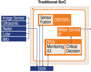
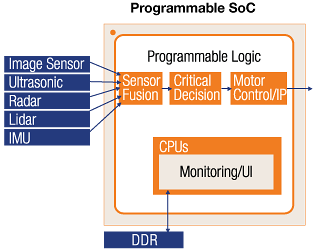
Figure 1: Comparison of a Traditional SoC and a Programmable SoC
Of course, as a system-on-a-chip, an inherent benefit of the use of a programmable SoC in place of a separate FPGA and processor system enables tighter integration, leading to improved size, weight and power - Cost (SWaP-C).
6. Structure of a Programmable SoC
As we saw in the introduction, a programmable SoC consists of many different structures; however, it can be split into two sections. These sections are the processor system (PS) and the programmable logic (PL).
The processor system, like its name suggests, contains the processors and associated interfaces. Typically, within the processor system, there will be the following elements:
- Processors: These are the heart of the processing system. Depending upon the architecture of the SoC, it may provide either a single processor core or, if multiple cores are present, they may be in either a homogeneous or heterogeneous configuration. One example of this is the Xilinx Zynq UltraScale+ MPSoC, which provides up to four Arm A53 processors and two Arm A5 processors in its processing system.
- On Chip Memory: This is memory connected to the processors from which applications can be executed. Depending upon the SoC and processor type, this may be all the memory required for the system. For more complex SoCs, OCM can be used for storing data, especially for Direct Memory Access (DMA) transfers.
- Cache: The cache structure will vary depending upon the complexity of the programmable SoC. Each processor will have its own small level one (L1) instruction and data cache. These individual processors will be connected to a larger level two cache (L2) for sharing data between processors. In more advanced programmable SoCs, Cache Coherent Interconnects (CCI) are provided, allowing the design elements within the PL to be implemented as either IO cache coherent or fully cache coherent. Cache coherence within the programmable SoC enables the shared data to be seen uniformly across the system. This prevents issues with stale cache data being used in one processing element of the SoC.
- Interfaces: The programmable SoC will be required to interface with several different commonly used interface standards. These will range from simple standards such as SPI, UART, and I2C, designed to interface with other devices and sensors, to more complex higher speed links such as Gigabit Ethernet and PCIe. Typically, a programmable SoC will provide IO bank(s) which can be connected to one of the several supported IO standards. This enables the programmable SoC processing system to optimize its use of IO standards—unused IO standards do not need to be routed out, allowing maximum flexibility.
- PS and PL Interfacing: To be effective as a programmable SoC, the PS and PL must be able to communicate. Depending on the application, the demands on the communication bandwidth will vary from low speed configuration and control to high bandwidth, cache coherent transfers. To facilitate this, Programmable SoCs provide a range of diverse communication interfaces. To support high bandwidth data transfer in both directions between PS and PL, high performance interfaces are required. Typically, these high-performance interfaces provide a range of options to enable the most efficient transfer, crucial for acceleration. These options include wide bus widths (32/64/128), Burst support, IO cache coherency, and connection to fast routing matrices to enable connection with high bandwidth memories and interfaces. While low bandwidth communications are provided by scaled-down versions of the high-performance interfaces, there are a number of different interfaces which could be used in a programmable SoC; some of the most popular include Arm eXtensible Interface (AXI) and Ultra Path Interconnect (UPI). However, in addition to the defined bus interface structures, other signals are also often required as well to cross the PS/PL boundary. These include interrupts (in both directions), Clocks & Resets from the PS, Debugging signals, and Dedicated DMA, along with streaming and event signals.
At this point, it is worth taking a deeper look at the AXI interface. AXI is part of the larger AMBA bus standard specifically tailored for ASIC/ FPGA/programmable SoC implementation. AXI is further split into three flavors:
- AXI Memory Map: This is an implementation of the full AXI memory mapped protocol and supports single address multiple data transfers. This is commonly used to implement DMA transfers between the PS and PL.
- AXI Lite: A simpler memory mapped interface which supports single address and single data transfers. This is commonly used to configure and control elements within the PL from the PS.
- AXI Streaming: This is a unidirectional protocol with no address channel, which streams data only. Streaming is commonly used between process elements in image processing chains or data paths.

Figure 2: AMBA bus standard

Figure 3: AXI Memory Mapped and AXI Lite. For AXI Memory Mapped and AXI Lite, the AXI interface implements separate read, write, and control channels.
When we connect AXI devices together, we do not connect them as a bus, but as point-to-point connections. If we wish to enable a single master to communicate with several slaves, we need to use an AXI Crossbar or interconnect structure.
The programmable logic half of the programmable SoC will contain predominantly logic cells and interconnects. However, as with all programmable logic, this will also include additional hard macros which further enable acceleration:
- Digital Signal Processing Units: These are highly optimized multiply-accumulate units which can also be used to implement the multiply-accumulates required for filter implementations. DSP units can also implement multiplication, addition / subtraction, and pattern matching and logical operations. DSP elements are very important structures in the PL when it comes to the acceleration of Filters, FFTs, and more, which are commonly implemented. If no dedicated multipliers were provided, then the structures would need to be implemented in the logic itself, which would give a slower overall performance.
- Block RAM (BRAM): These RAM elements can be configured. Trading address space for data width, several can be combined to create larger RAM structures. These are used in the programmable logic to implement single and dual port memories along with FIFO structures. When it comes to implementing our algorithms within the programmable logic, BRAMs and FIFOs are essential to providing the ability to buffer data between processing stages.
- Dedicated Hard Macros: Increasingly, programmable SoCs include dedicated hard macros within the programmable logic. These include PCIe, 100G Ethernet, Video Codecs, Forward Error Correction, and more. Typically, hard macros implemented within the PL are those that require high bandwidth input and output, which cannot be easily supported in the processing system.
- Mixed Signal Elements: One popular application for programmable SoCs is communication systems, like those which use Radio Frequency for communication / information gathering. Some programmable SoCs include mixed signal converters, which integrate the signal chain within the SoC itself. Examples of this include the Xilinx RFSoC, which includes Multi Giga Sample Converters.
7. Developing for a Programmable SoC
The development of a programmable SoC requires the use of both traditional software and FPGA development techniques. Depending upon both the complexity of the SoC and the end-application, the software development process will vary considerably.
Within a programmable SoC, the PS will be the master and will configure the PL following boot. This allows the processing system to be able to update and reconfigure the PL on the fly during run time. This means several different bit streams can be loaded as required, which is very useful for the acceleration of algorithms.
Following successful power-on tests, the SoC will attempt to configure by looking at its configuration memory to find a boot header and the boot loader. This initial boot loader will be the first stage boot loader (FSBL). The FSBL configures the system and allows configuration of the PL if desired, and then loads either the application or a second stage boot loader. The second stage boot loader (SSBL), such as UBoot, is used when a more complex operating system is being deployed, for instance embedded Linux.

Figure 4: Programmable SoC Configuration Process
The simplest applications will use a bare-metal development, which contains no operating system. Typically, when working with a programmable SoC, the device manufacturer will supply several Application Processing Interfaces (APIs) and libraries which can be used to interact with the elements in both the PS and the PL. This board support package will need to be regenerated each time the design is updated to include or remove new elements.
For more complex applications, an operating system is used; the type of OS selected will depend upon whether a real-time response is required or not. If a real-time response is required, then an operating system such as FreeRTOS or Micrium OS/III may be required. If a real-time response is not required, but the application requires working with high level frameworks and networking, then embedded Linux is a popular OS choice.
At this point you may be asking: "What differentiates a real-time operating system from one which is not?" An RTOS is deterministic. That means the response of the system will meet a defined deadline. However, failure of the RTOS to meet this defined deadline does not always mean it has failed. This depends upon the type of RTOS implemented.
There are three types of RTOS, which are as follows:
- Hard RTOS: Missing a deadline is classified as a system failure.
- Firm RTOS: Occasionally missing a deadline is acceptable and is not classified as a failure.
- Soft RTOS: Missing a deadline simply reduces the usefulness of the results.
Of course, the type of RTOS implemented within the programmable SoC depends upon the use case and requirements.
If the developer chooses bare-metal or FreeRTOS / Micrium, then development will be using C / C++ languages. If a higher-level operating system such as Linux is used, then the development language will depend upon what is being developed. If a Kernel driver is being developed, the developer will use C, as that is what the kernel is written in. However, if the developer is working within the user space, then a range of languages may be used, from C to Python and beyond.
The PL section of the programmable SoC is programmed using pre-supplied IP cores and custom IP created with Hardware Description Languages. Increasingly, High-Level Synthesis (HLS) is being used to reduce the complexity of designing custom IP by enabling developers to work in C and C++ (the same language commonly used for programming the processing system). This ability to generate programmable logic designs using HLS has enabled the development of system optimizing tools for programmable SoCs. System optimizing tools such as the Xilinx SDSoC Development Environment enable the entire design to be developed in C or C++ and run initially on the processing system to verify the functionality is as desired.
Once the functionality has been proved acceptable, the application can be profiled, and functions which require significant processing time can be accelerated in the programmable logic. When a system optimizing compiler is used, the movement from the PS to the PL is seamless, thanks to HLS and a connectivity framework which connects the accelerated functions into the processor memory.
System optimizing tools can be used with both a hard and soft programmable SoC approach.
8. Multiprocessing and Hypervisors
Typically, a programmable SoC provides several processing elements consisting of either homogeneous or heterogeneous processors. How we deploy and configure these multiple cores is called multiprocessing.
At the highest-level, multiprocessing is broken down into two distinct groups depending upon how the processors and the operating systems are combined. They are:
- Symmetric Multi-Processing: In an SMP application, all processors and resources are under the control of a single operating system.
- Asymmetric Multi-Processing: In an AMP application, multiple operating systems are used on different processors cores. All operating systems share the same physical system memory.
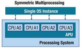
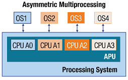
Figure 5: Comparison of a Symmetric and Asymmetric Multi-Processing Core
Using an AMP approach allows the programmable SoC to get the best of both worlds, combining real-time operating systems and application operating systems such as Linux.
Keep in mind, the choice of AMP or SMP is not dependent upon if the SoC is homogeneous or heterogeneous.
Of course, if we are using an AMP approach, then we need to be able to communicate and share resources between the different operating systems. Ideally, we want to be able to do this using a standard framework that allows us to manage both the life cycle and communications between different operating systems. If we do not use a standard framework for this, we will be re-inventing the wheel each time different processors are required to work together; this is costly both in non-recurring engineering effort and timescales.
One such framework is OpenAMP from the Multicore association. OpenAMP provides the framework for different operating systems to communicate and manage lifecycles as required. When OpenAMP is used within a programmable SoC, a typical deployment would be a Linux operating system managing the lifecycle and establishing the communication channels with other cores running different operating systems, for example, bare-metal or FreeRTOS.
The key elements of the OpenAMP framework that enable the above are:
- virtIO: Virtualization, which allows communication with the network and device drivers.
- remoteProc: This is the API that controls the remote processor. It starts and stops the execution, allocates resources, and creates the virtIO devices. This API performs what is often termed as the Life Cycle Management (LCM) of the remote processor.
- RPMesg: The API that allows inter-process communication between the master and remote processor.
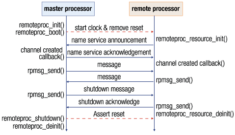
Figure 6: OpenAMP Flow between master and slave
However, if we use an OpenAMP approach on a programmable SoC, then each operating system has access potentially to the entire system resources and memory.
For some applications which are safety or security critical this may not be acceptable; as such, we need a different approach. In this instance, a hypervisor is often used. A hypervisor sits between the processor cores and several different virtualized operating systems. Due to how a hypervisor functions, each operating system running on the hypervisor believes it is the only operating system running on the hardware.
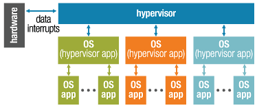
Figure 7: Hypervisors
Using a hypervisor enables the developer to allocate resources and enable access to system resources only as required. This provides for increased robustness and security in the end-application.
There are two types of hypervisors. Type-one hypervisors are configured by hardware and there is no software between the processors and hypervisor, while type-two hypervisors are run on a host operating system. One example of a type-one hypervisor is Xen, while an example of a type-two is Virtual Box. Both are commonly used in the development of programmable SoCs, with Xen being used on the programmable SoC itself and Virtual Box being used by developers to create Linux images depending upon their development environment.
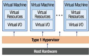
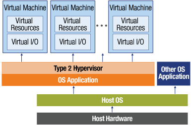
Figure 8: Comparison of the application of Type-One and Type-Two Hypervisors
9. Safety & Security
Increasingly, programmable SoC based solutions are deployed in applications where safety and security are required. While safety and security may share many similar design techniques, they are not the same. Safety in an embedded system context is ensuring the system is fully operational and protects the user. Security in an embedded system context is ensuring the data stored within the system is secure, protecting the data.
How security and safety errors are handled is also different. Should a safety error occur, this may or may not be correctable. If it is correctable, the error must be corrected, if not, then the system must fail in a safe manner. Should a security error occur within the system, then the system should be locked down immediately.
There are many different safety standards in use (e.g. IEC61508, IS26262, etc.). Many of these define safety levels, as is the case with IEC61508 and its Safety Integrity Level. The SIL level represents the level of protection against a failure occurring when compared to the risk of the failure occurring which is not detected or mitigated.
| SIL 1 | SIL 2 | SIL 3 | |
|---|---|---|---|
| PFH [1/h] | <10-5 | <10-4 | <10-7 |
| SFF (HFT=0) | >=60% | >=90% | >=99% |
| SFF (HFT=1) | - | >=60% | >=90% |
Figure 9: IEC61508 and Safety Integrity Levels
Implementing safety-related functions within a programmable SoC, therefore, requires the ability to ensure the device is functioning correctly and removing common cause failures.
Typical techniques which will be implemented within a programmable SoC intended for use in safety applications will include built-in self-test, monitoring of supply voltages and device temperatures, provision for Error Correcting Codes on memories, and the lock stepping of processor cores. Within the programmable logic section, further design features may also be implemented, such as redundancy, voting, ECC, and isolation of functions.
Check out this Tech Spotlight article on Functional Safety to learn more about this topic.
10. Simulation & Verification
Programmable SoCs are complex systems to verify and to debug, thanks to the combination of the processors and programmable logic. Many times, we need to be able to simulate or verify the interaction between the processing system and the programmable logic sections. Of course, debugging techniques vary from device to device; however, the concepts employed are similar.
One of the first things we may want to do in the programmable SoC development cycle is to test if the application software or operating systems will successfully boot. To simulate this in the first instance, we do not need to have access to the hardware; instead, we can use QEMU. QEMU is an open source software emulator capable of emulating most commonly used SoC processors, such as the Arm A53, Arm A9, Power PC, and MicroBlaze.
Using QEMU initially frees up the developer from needing access to the hardware, thus enabling a faster development cycle. However, as QEMU is an emulator, it cannot be used for a performance estimation.

Figure 10: Example Test Bench Structure
The typical development cycle for programmable logic will use an RTL simulator. Using this simulation tool, test benches will be developed which wrap around the PL module. This test bench will apply stimulus to the Unit Under Test and monitor the outputs to ensure they are in-line with the specification.

Figure 11: Example of Boundary Conditions and Corner Cases
The test bench will attempt to hit corner cases and boundary conditions of the unit. A boundary condition is when one of the inputs is at its extreme value, while a corner case is when all inputs are at their extreme value. A good example of this is illustrated by a simple 16-bit adder, which adds two numbers and produces a result. In this case the boundary condition and corner cases are illustrated in Figure 11.
Increasingly, simulation tools are enabling co-simulation between the QEMU and HDL simulation tools. This enables the real interaction between the application software and the programmable logic to be verified. This is achieved using QEMU coupled to the simulation tool; the connection between the QEMU and Simulation tool uses System C TLM.
Within the PL, manufacturers will also provide soft IP cores that can be integrated within the programmable logic. One commonly provided IP core, which is very useful, is an Integrated Logic Analyzer. This allows the states of internal signals to be captured and viewed over the JTAG Link.
When it comes to commissioning programmable SoCs, we need to be able to debug interactions between the PS and PL at run time. We can use breakpoints to halt the software, so that we can examine values in memory and registers. We can also use Integrated Logic Analyzers (ILA) to examine designs within the PL. What we need is a method to allow software break points and PL ILAs to work together to provide maximum information about the system’s behavior.
*Trademark. Xilinx is a trademark of AMD Corp. Other logos, product and/or company names may be trademarks of their respective owners.
Shop our wide range of SoCs, EVMs, application specific kits, embedded development boards, and more Shop Now.
Test Your Knowledge
Programmable Devices 2
Are you ready to demonstrate your Programmable SoCs knowledge? Then take a quick 15-question multiple choice quiz to see how much you've learned from this module.
To earn the Programmable Devices II Badge, read through the module to learn all about Programmable SoCs, attain 100% in the quiz at the bottom, and leave us some feedback in the comments section.



Top Comments
-

yuricts
-
Cancel
-
Vote Up
+1
Vote Down
-
-
Sign in to reply
-
More
-
Cancel
Comment-

yuricts
-
Cancel
-
Vote Up
+1
Vote Down
-
-
Sign in to reply
-
More
-
Cancel
Children