Take the Poll | Join our Discussion
sponsored by

Have You Ever Wondered How Vibrations Impact PCB-Mounted Electronic Components?
Electronic components in automotive, transportation, and industrial automation applications are constantly subjected to vibrations and shocks. In high vibration environments, or even during their manufacturing, printed circuit boards (PCBs) can suffer deformation, damage, and fractures, leading to outright failures or reduced life expectancies. While the risk is mitigated by the use of anti-vibration mountings, additional protective measures can be taken to prevent the failure of small electronic components.
This Tech Spotlight article explores potential problems multilayer ceramic capacitors experience in high stress environments, and countermeasures to prevent these problems.
Let’s Do a Brief Review: What Is a Multilayer Ceramic Capacitor (MLCC)?
Capacitors use electrical fields to store electrical energy. A simple capacitor consists of a pair of electrodes separated by a dielectric (Figure 1). The same structure is repeated in a compact Multilayer Ceramic Capacitor (MLCC) in successive levels to increase the stored charge. MLCCs have a broad capacitance range, making them ideal for many applications, including noise filters and power supply voltage smoothing.
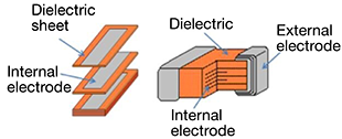
Figure 1: Basic structure of a monolithic ceramic capacitor
Image Source : Murata Manufacturing
MLCCs also have impressive high-frequency characteristics. The multilayer structure has less resistance compared to other capacitors. The low impedance of the ceramic capacitor benefits noise removal and enables the configuration of high-performance filters.
How Are MLCCs Damaged by Mechanical Stress and Strain?
MLCC chips are particularly susceptible to strain cracks. Because of the excessive mechanical force in high vibration environments, cracks due to mechanical stress and strain are inevitable. Figure 2 illustrates a strain crack that extends diagonally from the end of an external electrode.
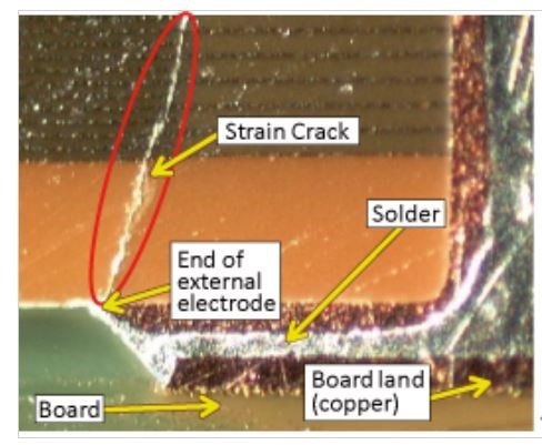
Figure 2: Example of a typical crack
Image Source: Murata Manufacturing
What Causes Strain Cracks?
The combination of thermal and mechanical stresses during mounting can cause strain cracks. During the process of soldering an MLCC to a PCB, mechanical stress is common. Excessive bending and twisting can cause cracks. Figure 3 shows the bending of a PCB where the top surface of the board becomes elongated, while the bottom surface is compressed. Cracks happen when such tensile stress exceeds the strength of the chip’s dielectric.

Figure 3: Board deformation and stress
Image Source: Murata Manufacturing
Why Does a Capacitor with a Strain Crack Fail?
Failures in MLCCs are mainly caused by the air gap that forms when a strain crack occurs. Air gaps can cause a variety of problems:
- Air gaps can cause a drop in capacitance.
- Severe air gaps can cause the capacitor to become an open circuit.
- Moisture or organic matter in the solder flux may enter the chip through the air gap, leading to lower insulation resistance.
In the worst cases, strain cracks can cause a short circuit. Figure 4 illustrates how cracks between the internal electrodes create a small air gap in the dielectrics between the electrodes.
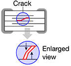
Figure 4: Dielectric Air Gap in Crack
Image Source: Murata Manufacturing
What Are the Common Countermeasures to PCB Stress and Strain?
PCB stress and strain can be a difficult problem to solve, due the varied sources of the vibrations. Stress and strain are often the result of mechanical resonances, which couple energy into the PCB (or the enclosure the PCB is mounted within), which builds up and causes displacements, leading to stresses that cause component failures. While the sources of vibrations are multi-faceted, the effects are well known: cracked capacitors, broken component leads, cracked solder joints, electrical shorts, and plated via barrel-to-pad separation. Common countermeasures to excessive vibrations on PCBs have included adding vibration isolators such as spring mounts or elastomer/neoprene shock mounts, among others.
How Does a PCB Designer Prevent Stress to Electronic Components?
In order to minimize the occurrence of strain cracks, countermeasures in process control and board design must be implemented. In process control, any processes where strain cracks commonly occur must be identified. Countermeasures can then be implemented.
From a board design perspective, the main preventative measures are the following:
- An appropriate distance must be present from the board edges, connectors, and screw holes.
- The layout and separation lines should generally run in parallel. Chips should not be placed near areas of high stress, such as corners and bends.
- In separation lines, slits are better than perforations.
- Land width for the chip must be less than the chip’s width. Figure 5 illustrates the land dimensions of a PCB, where dimension C is the chip's land width.
- The land pattern should be designed to prevent any deformation of the PCB during reflow soldering.
- In areas that might experience high strain, components that contain resin in the external electrode should be specified.

Figure 5 : Land dimensions
Image Source: Murata Manufacturing
| What does “Land” refer to on a PCB? A land (or pad) is the conductive area where a component is physically attached and electrically connected. A land pattern or footprint is the arrangement of the lands. |
Stress Testing a PCB
JIS C 5101-1-1998 is the deflection standard that evaluates the substrate deformation (bending) tolerance of an MLCC. Figure 6 illustrates the testing method used to evaluate an MLCC based on this standard. The test involves bending the PCB to a particular depth. The capacitance is measured, with the test revealing any defects.

Figure 6: Testing Method
Image Source: Murata Manufacturing
Typically, when a PCB is bent, tensile stress is focused on the external electrode. Figure 7 illustrates the distribution of the tensile stress caused by the bending of a PCB.
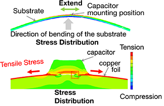
Figure 7: Stress Distribution
Murata KCM/KCA Series: Protecting Against Mechanical Stress with Flexible Metal Terminals
The Murata KCM series is a metal terminal type MLCC that incorporates flexible metal terminals to protect against mechanical stress. The metal terminals have an elastic action that flexes with the PCB, cushioning the capacitor from shocks and vibrations. The elasticity helps to reduce mechanical stress directly on the chip.
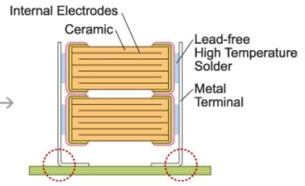
Figure 8: Mechanical stress is reduced by the elastic action of the MLCC’s flexible metal terminals.
Image Source: Murata Manufacturing
The KCM series remain undamaged even with a 6 mm board deflection, and solder cracks do not occur even after 2,000 cycles of heat stress. Audible noise is also substantially reduced.
KCM series capacitors are available in rated voltages of 25Vdc - 1000Vdc and capacitance from 8200pF to 100Μf. Sizes range from 6.1 x 5.1mm to 6.1 x 5.3mm.
KCA Series capacitors are IEC 60384-14 certified metal terminal type MLCCs for automotive use. They are suitable for duties as AC power line filters in battery chargers or DC line filters of DC-DC converter/inverter units. The KCA Series has a rated voltage of 250Vac (RMS) with capacitance from 100 - 10000pF. The size of the KCA Series is 6.1 x 5.1mm.
KCM55QR71J106KH01K, KCA55L7UMF221KH01L, and KCM55L5C2J183JDL1K are examples of KCM and KCA Series capacitors. Both series can be stacked for larger capacity.
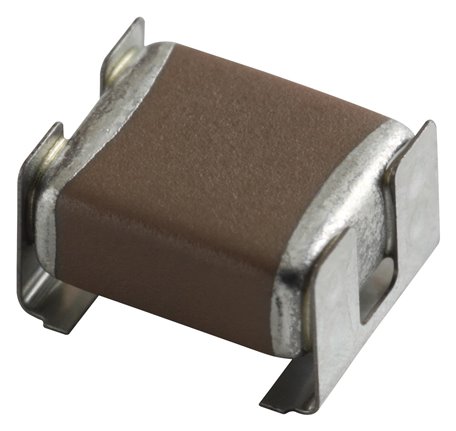
Figure 9: Murata Multilayer Ceramic Capacitor, 10 µF
Buy Now
MLCCs
Shop our wide variety of vibration absorbing MLCCs by Murata electronic components.
Don't forget to take our poll.
The following MLCCs from Murata employ the same metal terminal technology with different features and specifications.
KRM Series: a metal terminal type MLCC for general purposes, such as smoothing and noise suppression of DC-DC converters. They are available in rated voltages of 16Vdc - 1250Vdc and capacitance from 8200pF to 100μF, in a range of sizes from 2.2x1.25mm - 6.1x5.3mm.
KC3 Series: a High Effective Capacitance and High Allowable Ripple Current metal terminal-type MLCC for automotive applications, such as drive system control of the engine ECU and safety devices. The KC3 Series is available in rated voltages of 250Vdc - 630Vdc and capacitance from 0.10μF to 2.2μF. The size of the KC3 Series is 6.1 x 5.3mm.
KR3 Series: a High Effective Capacitance and High Allowable Ripple Current metal terminal-type MLCC for general purposes, such as DC-DC converters of general electronic equipment. The KR3 Series is available in rated voltages of 250Vdc - 630Vdc and capacitance from 0.10μF - 2.2μF. The size of the KR3 Series is 6.1 x 5.3mm.
Let’s Recap: How to Prevent MLCC Damage by Mechanical Stresses
Electronics components can suffer from mechanical bending, noise, or solder cracks in environments with high vibration and potential impacts. This mechanical stress in MLCCs can lead to strain cracks, leading to failure in other circuit components as well as the MLCC itself. Preventing damage caused by mechanical stress is a multilayered approach, which includes process flow and PCB design. In their KCM and KCA Series of MLCCs, Murata uses flexible metal terminals as an effective technique to cushion the MLCC from the stresses of vibration and shock.

-

dychen
-
Cancel
-
Vote Up
0
Vote Down
-
-
Sign in to reply
-
More
-
Cancel
-

kkazem
in reply to dychen
-
Cancel
-
Vote Up
0
Vote Down
-
-
Sign in to reply
-
More
-
Cancel
Comment-

kkazem
in reply to dychen
-
Cancel
-
Vote Up
0
Vote Down
-
-
Sign in to reply
-
More
-
Cancel
Children