


ReRam layers via Samsung
All flash memory has a finite number of guaranteed write/rewrite times. Some older and cheaper types are set at 100,000 and more advanced have 1,000,000. Using this type of memory as a solid state harddrive could push the memory to its breakdown phase fairly quickly with the constant disk access seen in most modern operating systems.
Researchers at the Samsung Advanced Institute of Technology are looking into creating non-volatile ReRam (resistive RAM) that is able to handle write cycles in the excess of 1,000,000,000,000 (1 trillion) at speeds (10ns) of up to a million times faster than current flash technology.
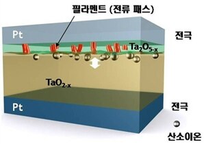
ReRam has dielectric properties. Normally insulating, but when energized it becomes conductive. Very much like a transistor gate, the memory element is a conductive path when its gate is closed. Apply the electrical spike and the gate opens, restricting current flow. Apply again, and the gate closes. Each bit of data holds its last state without power. Past ReRam was a tantalum film (Ta2O5 ). The Samsung researchers use a bi-layer structure of Ta2O5-x/TaO2-x filaments. This new bi-layer ReRam allows for more data to be set through the filament paths.
The IMEC consortium, a collection of the biggest technology companies, is behind this research. Member companies like HP, Intel, Panasonic, and, of course, Samsung want to explore and advance nano-electronics. Although this bi-layer ReRam looks promising, it is still several years away.
Eavesdropper

