


This blog grew out of my getting interested in wideband voltage amplifiers as a result of
doing the transistor load. Something that's fascinating with all this blogging is that,
whatever subject I choose to cover, it naturally seems to lead on to other related material
to explore and experiment with.
With the transistor load, a voltage amplifier formed part of the circuit. That controlled a
MOSFET to adjust the output current, with overall feedback to keep the current accurate. The
overall feedback was essential because the characteristic of the MOSFET at low currents is
quite non-linear and needs to be linearised by the feedback and also, given the kinds of
currents being controlled, temperature changes would also affect the response if the
feedback weren't there to remove them [even with the feedback, the current moved around
quite a lot due to heating in the current sense resistor which it couldn't account for]. An
evident disadvantage of having a multi-stage amplifier with very high open-loop gain and
overall feedback, for all its advantages in terms of precision and accuracy, is that it has
an impact on the closed-loop bandwidth that can be achieved because of the difficulties of
maintaining stability without rolling off the response early.
An alternative approach is to move to having [reasonably] precise feedback locally for each
gain stage, with each having fairly modest gain.
The circuit I'm going to look at here comes from a book by T O'Dell. He published this pair
of books as texts on circuit design about 30 years ago.

They are an interesting try at teaching actual design - how a designer pieces-together a
circuit to do a job. (Note that they aren't 'cookbooks', so if you want complete projects to
build they aren't for you, and neither are they text books, so you won't learn a lot of
basic theory.) Each chapter introduces a topic, discusses possible approaches, and then
leads on to an experimental circuit that could be built and experimented with. Sometimes
there are a couple of related topics in a chapter. The first book [1] (on the left in the photo
- mine is an ex-library copy which is why it is a bit scruffy) is a scatter of different
subjects, but for the second [2] he based it on the theme of test instrumentation and a fair
proportion is inevitably based on how the various sub-systems of a traditional analogue
oscilloscope would have been designed. Because he was targeting education, where the test
equipment then might not have extended to much more than a fairly modest 'scope, his
circuits were often slow versions of the real thing. One problem, though, I've found with
trying to work with the books now is that some of the integrated circuits he uses are no
longer available. This circuit is from the chapter where he discusses the kind of vertical
pre-amplifier that might have been used in an oscilloscope after the FET input stage but
before the high voltage plate-drive section. It's simplified and has limitations but it
allows some basic circuit ideas to be explored, which is what I'm going to do here.
How it Works
Here's the circuit as I've drawn it in the simulator

Although it's his circuit (more or less - I left out the zero adjustment and just tied the
other input to ground through a 47R resistor), they are my component values and aren't
necessarily very good, though it works in the simulator.
Although I'm learning and still not very good with some of this, let's see if I can explain
what is going on (feel free to point out anything that's wrong in the comments below).
There are two ways we can get local feedback with a transistor in order to stabilise the
gain and move it away from the very variable transistor properties: series feedback and
shunt feedback.

The series feedback stage is basically a transconductance amplifier - voltage in, current
out - and the shunt feedback stage is a transresistive stage - current in, voltage out.
[Trans-resistor is where the name 'transistor' comes from, though in some ways it might have
been more appropriate to call it a 'transductor'.] I haven't drawn the second one very well
as I've labelled the base current rather than the current at the input which would be in the
other direction.
An obvious thing to do with this pair is to join them together, so in this circuit both are
used in two successive stages. The first differential stage (T1 and T2) uses series
feedback, developed over R1 and R2 for each respective input transistor. The second stage
uses shunt feedback, utilising R9 and R10 for each of T3 and T4. The amplifier output is
differential, between the two collectors where I've placed a voltmeter on the schematic (but
for the traces below I looked at the output single-ended just by probing the collector of
T3). The differential output amplitude is twice that of the single-ended output. As an
amplifier for an oscilloscope, working with a differential output was natural because,
ultimately, after further amplification, this would be driving a pair of plates within the
tube in order to steer the electron beam.
T1 and T2 both have an input signal applied to the base and the output is taken from the
collector, so they are each in a common-emitter configuration (the emitter is common to both
input and output). [Although, for the purposes of the experimental circuit, T2 has no actual
input connected and is just tied to 0V, pretend that it's an input for this explanation.]
By swapping to NPN transistors for T3 and T4, the dc level can be folded back towards
ground, rather than wandering off and requiring higher and higher supply voltages for
multiple stages.
The small-signal performance looks fairly good in the simulator. Here's a frequency response
plot:

It's flat up to about 1MHz and the -3dB bandwidth is about 50MHz. The real circuit won't
manage that because of parasitic capacitances, but it's an indication of how it's making
reasonably good use of the raw 300MHz fT of the transistors.
I don't have a signal generator that I can look at that with, so instead I'm going to focus
on the large-signal response and how it gets on amplifying a square wave at a relatively low
frequency (1MHz).
Performance on a Circuit Board
To see how the circuit behaves, I've built it on a scrap of single-sided PCB material.

The centre strip is 0V, and the top and bottom strips are +15V and -15V respectively.
Normally I use a craft knife to cut the V-shaped groove to separate the different areas, but
this time I stupidly decided to have a go with a hacksaw blade and you can see the mess I
made of the upper cut before I reverted to the knife to finish the cut and do the other one.
The layout is more or less the same as the schematic. The large metal component that stands
above the first pair of transistors, to the left of the board, is the capacitor between the
emitters. This is a trimmer removed from some old radio chassis and has a range of about 10
-35pF, which is ideal for what I want to do here, and means I can see the effect of varying
the capacitance - more on that in a moment. The gungy brown material on the top is the
remains of a hard, waxy substance that was used to hold the position of the trimmer cap
after it had been set in the original circuit.
The input signal is connected to a BNC socket just off the left of the photo - the twisted
pair then brings it to the 47R resistor and the base of the transistor. Other than that,
there is just some decoupling for each rail (a 10uF electrolytic and a 100nF ceramic). For
the output I can just probe straight on to the resistors.
So how does it perform with a signal going in?
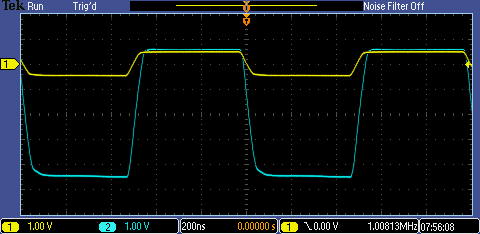
Here it is with a 1V pk/pk square-wave input [yellow trace] at approximately 1MHz. The
output [blue trace] is ac coupled and the capacitor has been trimmed for what I considered
the best wave shape. This is the waveform at one of the output collectors viewed singled-
ended with respect to ground [I chose the one that is in phase with the input].

Here is the positive edge in more detail
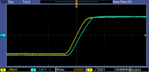
The gain is slightly over five. It follows the input quite nicely, with a delay of about
15nS, but can't quite keep up. The wave shape at the top where it comes in to land is
reasonable - it's just a fraction underdamped.
Here it is on the falling edge.
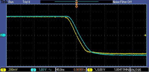
The reason it's a bit of a mess at the bottom is because it's faithfully following the input
from my cheap function generator which is also a bit of a mess.
What's the effect of changing the capacitor value?
Here it is with the capacitor set to a capacitance less than what I considered the optimum
value

and here it is with the capacitance larger

For me, this was a bit counter-intuitive; initially, I expected that more capacitance would
damp the response but it's the other way around. That's because the capacitor is on the
feedback. I'm not exactly sure about this, but I think that, with the fast edge, it
momentarily delays the feedback and allows the transistor to operate more as though it were
a simple common-emitter stage with a higher gain. That then gives more current to charge the
base-collector capacitance and improve the slew rate for large signals. So the capacitor
isn't there for stability, instead it's improving the way the circuit behaves with large
signals. (Unfortunately, having spent too much time looking at stability of circuits in the
simulator, I tend to see everything in those terms.) With too little capacitance we get the
basic response of the transistor, with too much it overshoots and is slow to return to the
feedback gain, and somewhere between is an optimum value where the two effects balance and
we get the best waveform shape. [Having thought about this a bit more, I think it must be having
to compensate for the base-collector capacitance of both transistors, the series feedback
one and the shunt feedback one.]
Biasing
The biasing, as I've done it, is far from ideal. For the above traces, I showed the output
ac-coupled. Here it is dc-coupled and you can see it isn't centred very well and extends
four-and-a-half volts below ground. That takes it down to the point where it's only a few
volts above the collector of the current source and almost straying into the area where the
transistor will no longer be able to hold the current steady.
Offsetting the input signal away from ground also has a bad effect. I imagine that that is
partly down to using a resistor for the tail current rather than a source.
It wouldn't be too difficult to correct the poor biasing - it is set by the tail currents
and the resistor values chosen for the collector load resistors - but I'm not going to do
that at the moment or the blog will never end.
Just be aware that, if you wanted to use it for real, it would need some further elaboration
and development.
If this blog interested you, a fairly comprehensive list of others can be found here: jc2048 Blog Index
[1] Electronic Circuit Design: Art and Practice. T. H. O'Dell. Cambridge University Press, 1988.
[2] Circuits for Electronic Instrumentation. T. H. O'Dell. Cambridge University Press, 1991.
Top Comments