


Introduction
More experimenting with MOSFETs. This time I'm going to have a look at the output characteristics.
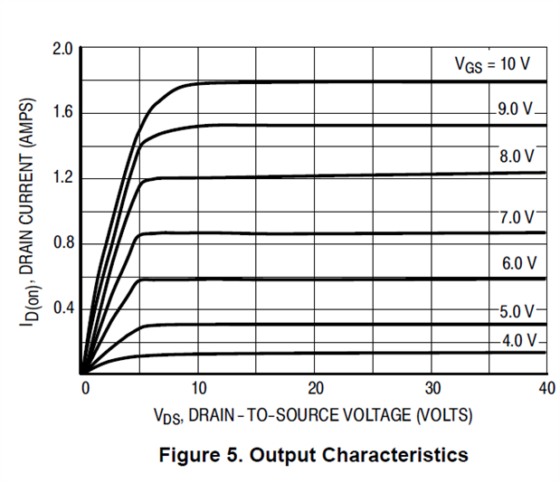
On a datasheet, output characteristics are usually drawn something like the following two graphs. The first is for the IRF730 part that I have been experimenting with extensively in this series of blogs and the second is for a small-signal part, a BS170:
Curves of drain current against drain-source voltage are drawn for a set of fixed Vgs voltages. The Vgs voltage step size is chosen to give a reasonable spread of curves and the choice will depend, in part, on the forward transconductance of the part: a power device, with a fairly high transconductance, will need the gate voltages closer [half volt steps seem to be common] than a small-signal part, like a BS170 or 2N7000, where the step size might typically be one volt.
For this blog, I'm going to try and display the curves for the BS170 part. Dealing with the kind of currents involved with the small part will be much easier than trying to do the same with a power transistor. The resulting graph will also show the active-region section of the curves, above pinch-off, better.
Circuit
Now I need to consider the design of the test circuit. As before, I'm going to draw the curves on the screen of my oscilloscope. That will enable me to do the test for each curve quickly, with a long rest period [10ms] in between tests, in order to get around the otherwise difficult problem of the very high level of dissipation once the drain voltage is fairly high and the drain current is also high.
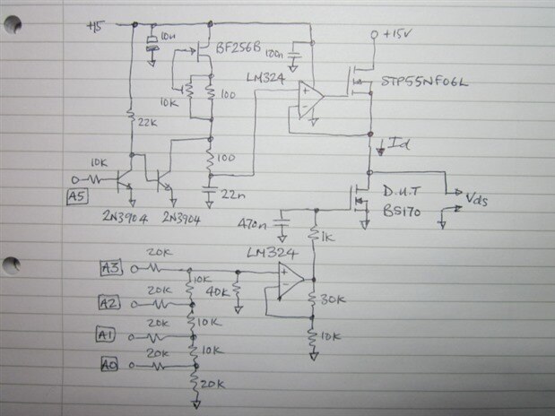
I need to be able to control the gate voltage so that it can be changed for each sweep. After a bit of thought, I decided to do this with a variant of the simple resistor-ladder DAC that I've used previously with an Arduino.
That's convenient because I'm also going to be using an Arduino UNO again to do the timing of the test. The ladder can only have an output within the 5V range of the UNO's power rails and wouldn't be able to drive the gate of the DUT [device under test] very hard, so I'm going to buffer it with an op-amp circuit with a gain of x4. That way, I get a range of 0-15V in 1V steps. Although it's far from ideal for this application, I'm going to see if I can get away with using a cheap LM324 device for this. With feedback, the op amp output has a low impedance [well below an ohm], but the natural output resistance of the amplifier will be tens of ohms, possibly as much as a hundred, so when the drain voltage starts rising, the internal intrinsic capacitances of the MOSFET might result in the gate moving around and the op amp won't necessarily be fast enough to counter it. To avoid any problems with that [I won't have problems with the BS170, I was thinking ahead to the situation if I try testing power devices], I'm going to have a 470n capacitor at the gate, isolated from the op amp output with a resistor. The 470nF is hundreds of times the size of any intrinsic capacitance and will reduce any disturbance at the gate in proportion. There is plenty of time between test intervals for the capacitor to charge to the new gate level, I just need to remember to write the new A/D value to the resistor ladder at the end of one test so that it has maximum time to settle before the start of the next.
The final thing I need to do is to find a way to vary the drain voltage whilst measuring the drain current. I going to try doing that with another MOSFET, wired as a source follower, controlled by an op amp with the JFET constant- current source that I used in one of the previous blogs charging a capacitor to give a reference voltage ramp for it to follow. That will be enabled for the 50us of the test by an output pin of the UNO.
The drain current I'll simply measure directly with a current probe. Plotting that against the voltage at the drain of the device will then sketch the curve.
Put all that together and this is the resulting circuit diagram:
rather than start again from scratch, as it already had some of the circuit on it, though that meant it all ended up a bit on the messy side.
The red/black leads [left] connect to the PSU that's providing the 15V for the MOSFETs. The yellow/orange leads are to a separate supply for the op amp and the ramp circuitry. The red loop at the bottom edge is for the current probe. The UNO is powered from its USB lead.
The upside-down chip is the op amp [it's not really dead, it's just pretending].
Testing a BS170
The code for the Arduino UNO was very simple. Note that it's specific to the UNO as I talk directly to the output pins to save time.
/* mosfet output-characteristic control program */

#include <arduino.h>

#define START_VOLTAGE 4
#define END_VOLTAGE 10

void setup() {
  PORTC = 0x00;
  DDRC = DDRC | 0x2F;    // set output pins
}

void loop() {
  int i;
  while(1) {
    for(i = START_VOLTAGE; i <= END_VOLTAGE; i++) {
      PORTC &= 0xFFF0;
      PORTC |= i & 0x000F;
      delayMicroseconds(10000);
      noInterrupts();
      PORTC |= 0x20;
      delayMicroseconds(50);
      PORTC &= ~0x20;
      delayMicroseconds(20);
      interrupts();
      }
    }
}
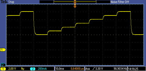
The code steps the gate voltage from 4V to 10V in one volt steps. For each step, there's a pause of 10ms and then it carries out the test for 50us by taking pin A5 high at the start and then low at the end. I'm using a long persistence on the oscilloscope to accumulate the separate curves, so that it will give me a graph like the one you'd see in a datasheet.
Here's the gate voltage as it's doing that. You can see the way it's being changed every 10ms and how it settles well before the next test
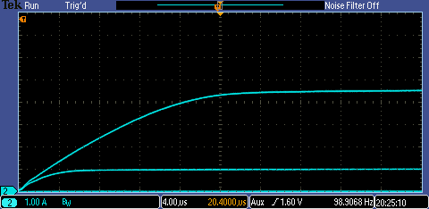
This next trace shows the Vds voltage in yellow and the Id current curves in blue. I've adjusted the drain voltage so that it sweeps from 0 to 10V in the width of the screen [ten divisions, so 1V/div]. That saves me from having to use the XY plot [which is very limited on this particular 'scope].
here it is again without the voltage curve
This nicely shows the shape of the curves. The bottom curve is for 4V gate drive, the top one for 10V, and the current is 500mA per division, so the top curve is exceeding 2.6A. My curves appear much smoother that the manufacturer's. The main deficiency of mine is right at the start where they get off to a slightly wobbly lift-off [that will be my test circuit, not the MOSFET]. The top two curves coming down again at higher voltages might be dissipation related (by that stage, for the higher one, the device is dissipating more than ten watts which will have some heating effect in a small die in a TO92 package, even when limited to just a few tens of microseconds).
Testing an IRF730
I was going to end there but couldn't resist trying the IRF730. Although it's a power device, the currents are manageable if I keep the Vgs fairly low, so I set the UNO to test at 5V and 6V. Here are the traces. This one closely matched the typical device on the datasheet.
Testing a BSS138
Finally, I thought I'd have a go at a BSS138. This has a lower threshold than the BS170, so I tested with steps from 2V up to 8V. Here is the graph I obtained.
Again, this one seemed to be better than the datasheet, but a major problem was the small package. For the first couple of seconds, the traces visibly move around before the temperature of the part stabilizes and everything comes to rest, so it certainly won't match the 25degC of the manufacturer's test.
Conclusions
That worked much better than I thought it would and, with a bit of work, could probably be turned into a piece of test equipment. The test isn't perfect, even with a pulse test (0.5% duty cycle) there is evidence of temperature effects, but it's nice being able to come up with reasonably plausible curves.
Other MOSFET Blogs
Experimenting with MOSFETS: Total Gate Charge Experimenting with MOSFETs: Transfer Characteristic Experimenting with MOSFETS: Threshold Voltage
If you found this blog interesting and would like to see others I've written, a list can be found here: jc2048 Blog Index |


Top Comments
-

genebren
-
Cancel
-
Vote Up
+3
Vote Down
-
-
Sign in to reply
-
More
-
Cancel
Comment-

genebren
-
Cancel
-
Vote Up
+3
Vote Down
-
-
Sign in to reply
-
More
-
Cancel
Children