element14 Community
element14 Community
    Register Log In
  • Site
  • Search
  • Log In Register
  • Community Hub
    Community Hub
    • What's New on element14
    • Feedback and Support
    • Benefits of Membership
    • Personal Blogs
    • Members Area
    • Achievement Levels
  • Learn
    Learn
    • Ask an Expert
    • eBooks
    • element14 presents
    • Learning Center
    • Tech Spotlight
    • STEM Academy
    • Webinars, Training and Events
    • Learning Groups
  • Technologies
    Technologies
    • 3D Printing
    • FPGA
    • Industrial Automation
    • Internet of Things
    • Power & Energy
    • Sensors
    • Technology Groups
  • Challenges & Projects
    Challenges & Projects
    • Design Challenges
    • element14 presents Projects
    • Project14
    • Arduino Projects
    • Raspberry Pi Projects
    • Project Groups
  • Products and Partners
    Products and Partners
    • Arduino
    • Avnet & Tria Boards Community
    • Dev Tools
    • Manufacturers
    • Multicomp Pro
    • Product Groups
    • Raspberry Pi
    • RoadTests & Reviews
  • About Us
    About the element14 Community
  • Store
    Store
    • Visit Your Store
    • Choose another store...
      • Europe
      •  Austria (German)
      •  Belgium (Dutch, French)
      •  Bulgaria (Bulgarian)
      •  Czech Republic (Czech)
      •  Denmark (Danish)
      •  Estonia (Estonian)
      •  Finland (Finnish)
      •  France (French)
      •  Germany (German)
      •  Hungary (Hungarian)
      •  Ireland
      •  Israel
      •  Italy (Italian)
      •  Latvia (Latvian)
      •  
      •  Lithuania (Lithuanian)
      •  Netherlands (Dutch)
      •  Norway (Norwegian)
      •  Poland (Polish)
      •  Portugal (Portuguese)
      •  Romania (Romanian)
      •  Russia (Russian)
      •  Slovakia (Slovak)
      •  Slovenia (Slovenian)
      •  Spain (Spanish)
      •  Sweden (Swedish)
      •  Switzerland(German, French)
      •  Turkey (Turkish)
      •  United Kingdom
      • Asia Pacific
      •  Australia
      •  China
      •  Hong Kong
      •  India
      •  Japan
      •  Korea (Korean)
      •  Malaysia
      •  New Zealand
      •  Philippines
      •  Singapore
      •  Taiwan
      •  Thailand (Thai)
      •  Vietnam
      • Americas
      •  Brazil (Portuguese)
      •  Canada
      •  Mexico (Spanish)
      •  United States
      Can't find the country/region you're looking for? Visit our export site or find a local distributor.
  • Translate
  • Profile
  • Settings
Community Hub
Community Hub
Member's Forum Datasheet confusion, re: layout instructions
  • Blog
  • Forum
  • Documents
  • Quiz
  • Events
  • Leaderboard
  • Polls
  • Files
  • Members
  • Mentions
  • Sub-Groups
  • Tags
  • More
  • Cancel
  • New
Join Community Hub to participate - click to join for free!
Actions
  • Share
  • More
  • Cancel
Forum Thread Details
  • Replies 14 replies
  • Subscribers 631 subscribers
  • Views 1499 views
  • Users 0 members are here
Related

Datasheet confusion, re: layout instructions

Andrew J
Andrew J over 7 years ago

Hopefully someone can take a look and help me get some insight into what is being stated.  This is in relation to layout of a DC-DC switching regulator LTC1624 (for my power supply build).  The data sheet, pages 20 and figure 9 on page 21, seem to conflict or, at least, not make sense in respect to the reference made to power and signal grounds.


Layout instructions state:

  1. Power ground and signal ground must be segregated.
  2. Ground pin of LTC1624 must return to -ve of Cout.
  3. The resistive divider must connect between +ve of Cout and signal ground
  4. Cin must connect to Vin and Ground of LTC1624

(I've summarised somewhat but that's the essential gist - they make reference to a POWER ground and a SIGNAL ground). 


Figure 9:

image

Looking at the layout figure 9, you can see that it follows these instructions and it would imply that -ve of Cout is signal ground; however this is directly linked to Schottky -ve pin, Cin-ve and back to the Vin - terminal


I've found a demo board for this chip. Unfortunately, the gerbers don't load into any viewer I can find, but there are images here on page 8 (last page.) 

Silk Screen:

image

Component Side (top):

image

Solder Side (bottom):

image


Looking at the Component Side (top) and Solder Side (bottom), there are two ground planes: a 'Z' like structure from Vin GND terminal E2, top left, under the LTC1624, to the Vout GND out terminal bottom right E5; the biggest copper area on Solder Side is Ground, also tied into E2 and E5.  I know 'Z' ground isn't a technical term but bear with me - I want to call it POWER ground but I'm not sure that would be right!  Looking at the Component Side silkscreen, it is clear Cout -ve is tied to the component side 'Z' ground; the feedback divider is also connected to the 'Z' ground where the sideways-U trace is.  It's worth noting also that the loop compensating resistor/capacitor is tied to the 'Z' ground.


Looking at Figure 9 and the PCB layout, it would seem that everything is tied into the same ground - it isn't clear if anything is tied into the ground plane on the Solder Side (except at terminals E2 and E5) and I've traced every component that has a ground connection to the Component Side 'Z' ground.  In other words, it's not clear what they mean by tying the resistor divider to signal ground. 


Anyone who has been following along with my build will know I've right-royally screwed up the grounding and layout and I don't want to do it again.  It's been clear that I've not fully understood how Switching Regulators work so I've been doing a lot of reading and now have a better idea.  I understand why the feedback divider should stretch across Cout so why it is tied to the -ve of Cout and figure 9 actually makes sense to me (except for the ground symbol under the Schottky plus a link to Vin GND.)  What doesn't make sense are the layout instructions reference to Power and Signal grounds and the layout of their PCB - it would seem that the way both the feedback and compensation components are tied to the ground plane, right by Schottky, would be inviting noise and poor behaviour.  It's also tying noise onto the Vout GND terminal as well.


I'd have to assume that the PCB layout is purely for the purposes of demonstrating the functionality of the LTC1624 and is less concerned with the quality of the output.  Thus, I would expect that I would tie the Feedback and LTC1624 grounds to Cout -ve along a different Ground route.  That would also be the point for tying downstream ground components (so basically, like Figure 9 where the Vout -ve is deemed signal ground and Cout -ve becomes the star ground point for signal.)


Is this clear to anyone else?

  • Sign in to reply
  • Cancel
Parents
  • shabaz
    shabaz over 7 years ago

    Hi Andrew,


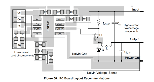
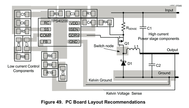
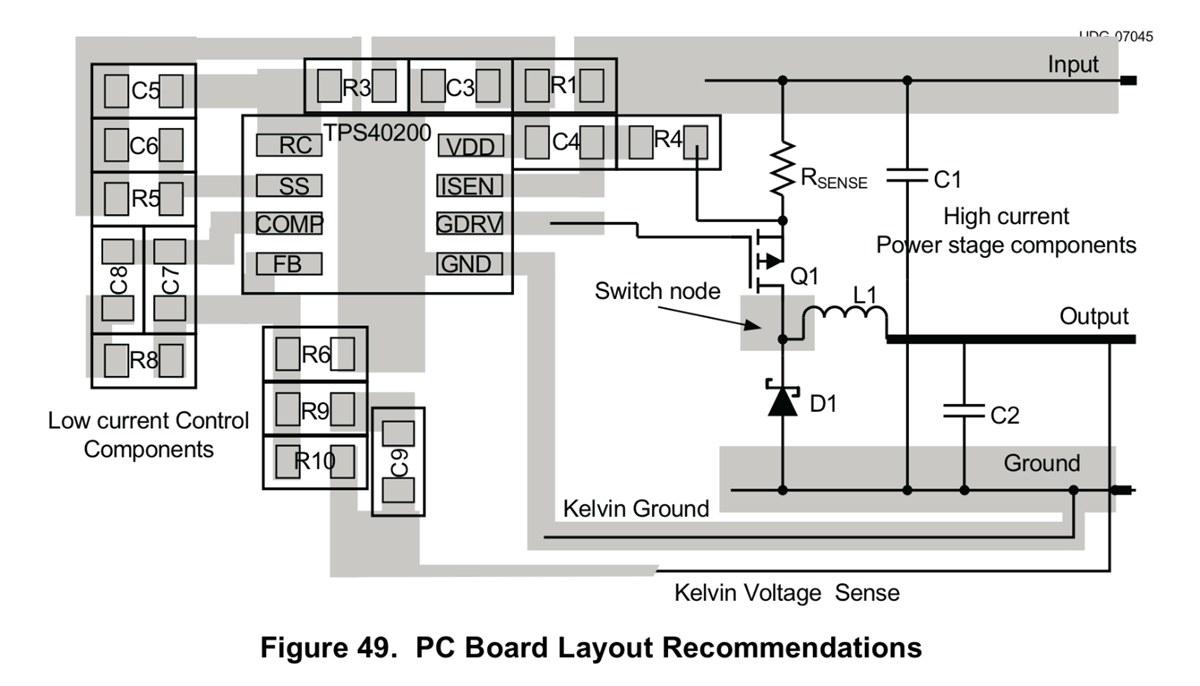
    I took a look at a different chip I've used in the past, just to see what the recommended layout is like. Here R10 and R6 form the feedback resistor divider:

    image

    Perhaps that can give some ideas. Also it could be worth querying from LT directly, letting them know that their datasheet makes no sense. They are responsive (I asked them a while back concerning some other chip).

    • Cancel
    • Vote Up +3 Vote Down
    • Sign in to reply
    • Cancel
  • Andrew J
    Andrew J over 7 years ago in reply to shabaz

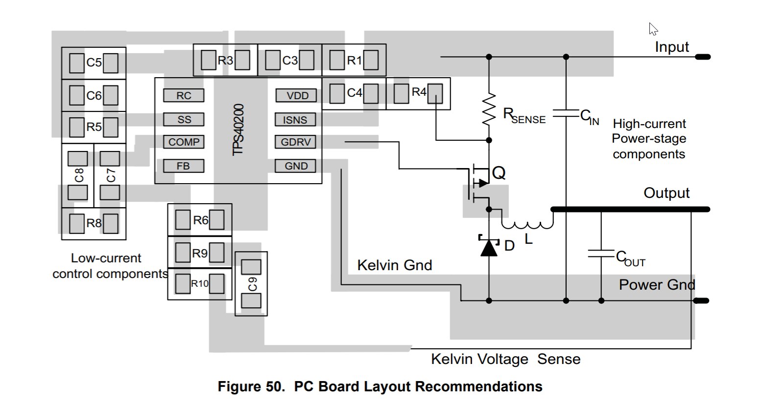
    That is helpful, thanks - I was trying to work out how the chip got power as VDD is connected through a capacitor and resistor, C4 and R4!  Checking the datasheet for the TPS40200, I think you must have an older version as it looks different in the version I saw.

    image


    Anyway, it is useful and if you compare the layout with Figure 9 for the LTC1624, they are pretty comparable.  In this version, we can see that GND pin is connected at the same point as the feedback divider (and compensation loop) at Cout (or C2 in this figure.)  That makes me think even more that the evaluation board layout was not done with quality output in mind, just capability.  I guess without getting hold of one I'll never know, but I will contact LT and see if they can clarify, good suggestion.  The layout notes in the TI datasheet are way clearer as well.


    Doing more research on DC-DC switchers has given me even more insights into how wrong my layout was in respect to ground.  Clearly I need to follow that high-current path all the way to the output terminals and consider the ground connections for the low current control components accordingly. 


    Can I ask two further questions:  in the TI datasheet it says "Traces carrying large AC currents should NOT be connected through a ground plane. Instead, use PCB traces on the top layer to conduct the AC current and use the ground plane as a noise shield."  Does this mean that the high current traces, including Ground traces, should be on the top layer with a solid ground plane underneath to which nothing is connected, except where ground routing on the top layer is impossible and needs to be routed on ground plane layer?  Here I'm imagining a 4-layer board with high current traces on top layer, then shielding Ground Plane (routed/split away from sensitive components), then signal ground plane, then signal traces.  Both shielding and signal ground planes connected at, where, Cout -ve? Vin -ve?

    • Cancel
    • Vote Up +4 Vote Down
    • Sign in to reply
    • Cancel
  • genebren
    genebren over 7 years ago in reply to Andrew J

    Andrew,


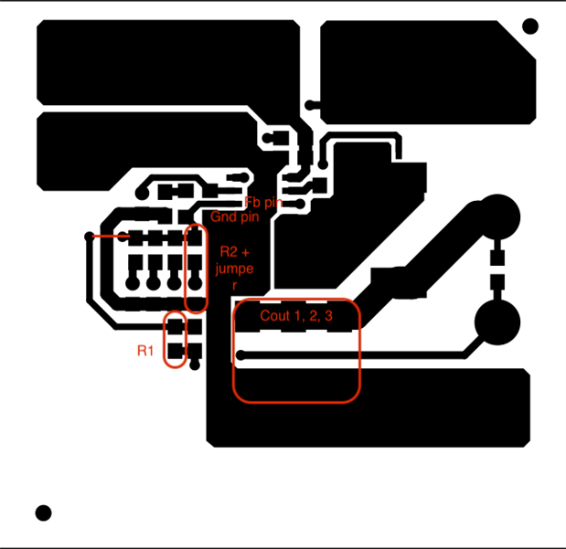
    Can I ask two further questions:  in the TI datasheet it says "Traces carrying large AC currents should NOT be connected through a ground plane. Instead, use PCB traces on the top layer to conduct the AC current and use the ground plane as a noise shield."  Does this mean that the high current traces, including Ground traces, should be on the top layer with a solid ground plane underneath to which nothing is connected, except where ground routing on the top layer is impossible and needs to be routed on ground plane layer? Here I'm imagining a 4-layer board with high current traces on top layer, then shielding Ground Plane (routed/split away from sensitive components), then signal ground plane, then signal traces.

    image


    image

    In the top image, the ground plane (both Kelvin Gnd and Power Gnd) are shown in a single trace.  In the lower image, the Ground and the Kelvin Ground are more of a starred arrangement, where the high currents are passed through the thick trace and the low currents through a separate (thinner) trace.  This is a simple start, but the situation gets much more complicated when the high and low currents are a part of the ground plane flooding, where the there is a lot of copper, but it begins to take on convoluted shapes and exists on multiple layers, inter-stitched.  Do the large paths need to be on the top layer?  Mostly yes, because that is where the components in the high current path are.  The most direct connection (trying not to use vias) is the preferred method of connection.  When thinking of a solid ground plane on another layer, again you need to be careful about the possibility of mixing high and low currents, so if you need to stitch connections, try and do it with traces and vias, not necessarily vias to a flooded plane.


    Both shielding and signal ground planes connected at, where, Cout -ve? Vin -ve?


    Tie them at a single point.  I usually tie traces at the input side (ve).  From the source side, I star out a low current path and a high current path, never allowing then to reconnect to each other.  If I am adding a ground plane (shielding), it is also connected to the ground at the 'star' point and again, never allowing it to reconnect to the other ground paths.


    Gene

    • Cancel
    • Vote Up +4 Vote Down
    • Sign in to reply
    • Cancel
  • Andrew J
    Andrew J over 7 years ago in reply to genebren

    Thanks Gene.  I’ll study this pic, and the other one you posted on this topic.

    • Cancel
    • Vote Up +1 Vote Down
    • Sign in to reply
    • Cancel
  • genebren
    genebren over 7 years ago in reply to Andrew J

    Andrew,


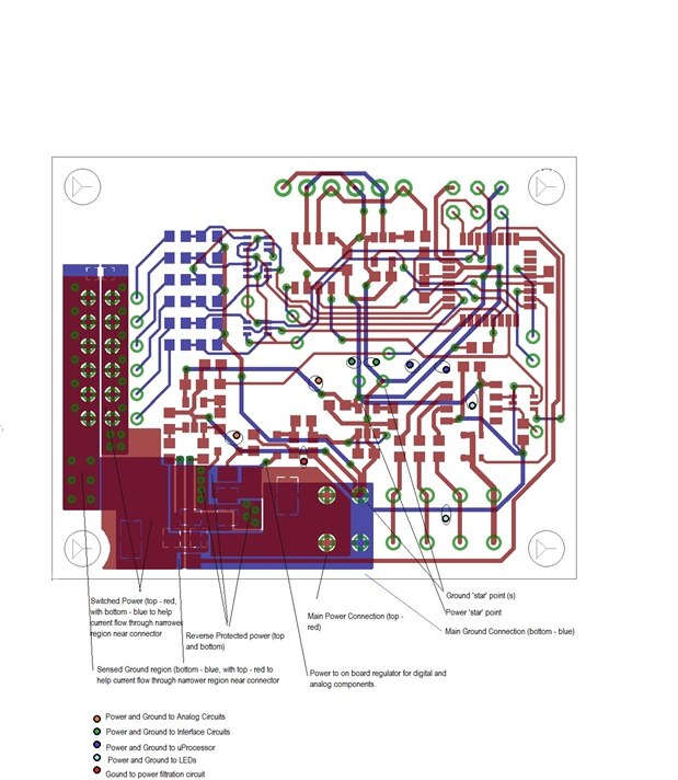
    The easiest way to avoid having ground loops is prevent having loops.  This is done by radiating the ground traces away from a single point (i.e. star pattern).  You also need to separate paths of high current flow from paths of low current flow (while not necessary a loop issue, what you are fighting here is noise, introduced by the IR voltage drop).  Here is an example from a board that I am currently working on.  This board supplies up to 8Amps to external servo (up to 6).  As a result, there are some hefty traces for power (quite noisy).  To isolate the remaining circuits from noise (from the power/ground paths) a lot of efforts were taken to purposely route power and ground to the rest of the board.


    image

    Gene

    • Cancel
    • Vote Up +1 Vote Down
    • Sign in to reply
    • Cancel
Reply
  • genebren
    genebren over 7 years ago in reply to Andrew J

    Andrew,


    The easiest way to avoid having ground loops is prevent having loops.  This is done by radiating the ground traces away from a single point (i.e. star pattern).  You also need to separate paths of high current flow from paths of low current flow (while not necessary a loop issue, what you are fighting here is noise, introduced by the IR voltage drop).  Here is an example from a board that I am currently working on.  This board supplies up to 8Amps to external servo (up to 6).  As a result, there are some hefty traces for power (quite noisy).  To isolate the remaining circuits from noise (from the power/ground paths) a lot of efforts were taken to purposely route power and ground to the rest of the board.


    image

    Gene

    • Cancel
    • Vote Up +1 Vote Down
    • Sign in to reply
    • Cancel
Children
  • Andrew J
    Andrew J over 7 years ago in reply to genebren

    Thanks Gene.  I’ll study this pic, and the other one you posted on this topic.

    • Cancel
    • Vote Up +1 Vote Down
    • Sign in to reply
    • Cancel
element14 Community

element14 is the first online community specifically for engineers. Connect with your peers and get expert answers to your questions.

  • Members
  • Learn
  • Technologies
  • Challenges & Projects
  • Products
  • Store
  • About Us
  • Feedback & Support
  • FAQs
  • Terms of Use
  • Privacy Policy
  • Legal and Copyright Notices
  • Sitemap
  • Cookies

An Avnet Company © 2026 Premier Farnell Limited. All Rights Reserved.

Premier Farnell Ltd, registered in England and Wales (no 00876412), registered office: Farnell House, Forge Lane, Leeds LS12 2NE.

Follow element14

  • X
  • Facebook
  • linkedin
  • YouTube