element14 Community
element14 Community
    Register Log In
  • Site
  • Search
  • Log In Register
  • About Us
  • Community Hub
    Community Hub
    • What's New on element14
    • Feedback and Support
    • Benefits of Membership
    • Personal Blogs
    • Members Area
    • Achievement Levels
  • Learn
    Learn
    • Ask an Expert
    • eBooks
    • element14 presents
    • Learning Center
    • Tech Spotlight
    • STEM Academy
    • Webinars, Training and Events
    • Learning Groups
  • Technologies
    Technologies
    • 3D Printing
    • FPGA
    • Industrial Automation
    • Internet of Things
    • Power & Energy
    • Sensors
    • Technology Groups
  • Challenges & Projects
    Challenges & Projects
    • Design Challenges
    • element14 presents Projects
    • Project14
    • Arduino Projects
    • Raspberry Pi Projects
    • Project Groups
  • Products
    Products
    • Arduino
    • Avnet Boards Community
    • Dev Tools
    • Manufacturers
    • Multicomp Pro
    • Product Groups
    • Raspberry Pi
    • RoadTests & Reviews
  • Store
    Store
    • Visit Your Store
    • Choose another store...
      • Europe
      •  Austria (German)
      •  Belgium (Dutch, French)
      •  Bulgaria (Bulgarian)
      •  Czech Republic (Czech)
      •  Denmark (Danish)
      •  Estonia (Estonian)
      •  Finland (Finnish)
      •  France (French)
      •  Germany (German)
      •  Hungary (Hungarian)
      •  Ireland
      •  Israel
      •  Italy (Italian)
      •  Latvia (Latvian)
      •  
      •  Lithuania (Lithuanian)
      •  Netherlands (Dutch)
      •  Norway (Norwegian)
      •  Poland (Polish)
      •  Portugal (Portuguese)
      •  Romania (Romanian)
      •  Russia (Russian)
      •  Slovakia (Slovak)
      •  Slovenia (Slovenian)
      •  Spain (Spanish)
      •  Sweden (Swedish)
      •  Switzerland(German, French)
      •  Turkey (Turkish)
      •  United Kingdom
      • Asia Pacific
      •  Australia
      •  China
      •  Hong Kong
      •  India
      •  Korea (Korean)
      •  Malaysia
      •  New Zealand
      •  Philippines
      •  Singapore
      •  Taiwan
      •  Thailand (Thai)
      • Americas
      •  Brazil (Portuguese)
      •  Canada
      •  Mexico (Spanish)
      •  United States
      Can't find the country/region you're looking for? Visit our export site or find a local distributor.
  • Translate
  • Profile
  • Settings
Community Hub
Community Hub
Member's Forum LED Construction
  • Blog
  • Forum
  • Documents
  • Quiz
  • Events
  • Leaderboard
  • Polls
  • Files
  • Members
  • Mentions
  • Sub-Groups
  • Tags
  • More
  • Cancel
  • New
Join Community Hub to participate - click to join for free!
Actions
  • Share
  • More
  • Cancel
Forum Thread Details
  • State Verified Answer
  • Replies 5 replies
  • Answers 2 answers
  • Subscribers 531 subscribers
  • Views 655 views
  • Users 0 members are here
  • light-emitting diode
  • electroluminescence
  • led
  • active region
Related

LED Construction

Anonymous-532400
Anonymous-532400 over 7 years ago

Hello,

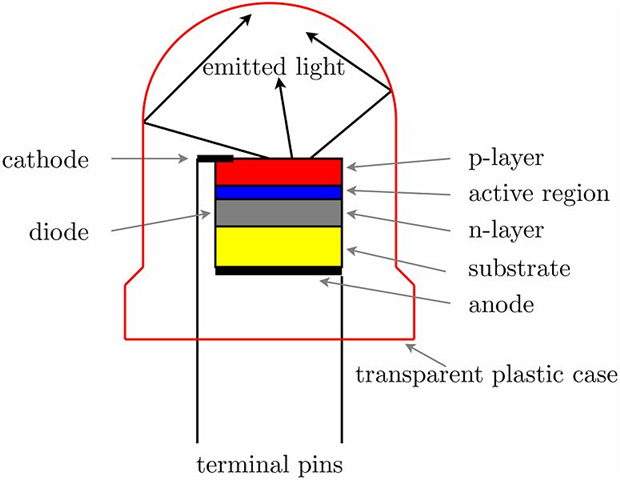
I was researching how an LED works, and came across two things that I can't seem to find any solid information on, the "active region", and the "substrate" of an LED.

So, if anyone could explain a little what these are and what they do, that would be appreciated.a


Light Emitting Diodes

  • Sign in to reply
  • Cancel

Top Replies

  • dougw
    dougw over 7 years ago +7 verified
    The active region is where photons are generated as electrons jump to a lower energy level across the diode junction. The substrate is un-doped semiconductor. The P layer is P doped semiconductor. The…
  • jc2048
    jc2048 over 7 years ago +6 suggested
    This is my understanding, but I may be a bit out of date with some of it and could be wrong in some of the detail. The substrate of most active devices (ICs, transistors, diodes, LEDs, etc) comes from…
  • dougw
    dougw over 7 years ago in reply to Anonymous-532400 +2 suggested
    The substrate is the starting wafer of semiconductor material before it has been processed to make diodes. The P-N layers are just the areas at the top of the substrate after it has had small amounts of…
  • dougw
    0 dougw over 7 years ago

    image

    The active region is where photons are generated as electrons jump to a lower energy level across the diode junction.

    The substrate is un-doped semiconductor. The P layer is P doped semiconductor. The N layer is N doped semiconductor. The N and P layers form a diode.

    • Cancel
    • Vote Up +7 Vote Down
    • Sign in to reply
    • Verify Answer
    • Reject Answer
    • Cancel
  • jc2048
    0 jc2048 over 7 years ago

    This is my understanding, but I may be a bit out of date with some of it and could be wrong in some of the detail.


    The substrate of most active devices (ICs, transistors, diodes, LEDs, etc) comes from the large, circular wafer of semiconductor material that the subsequent processing steps are done to. In the very early days other methods were used, but now wafer processing dominates (because it lends itself to handling the fabrication of large numbers of devices in an efficient way).


    The n-type layer is formed in the substrate by gas diffusion in an oven (doping) or, for the kind of IC where the features need to be very small, ion implantation from an ion beam. Then the p-type region is diffused into the n-type. Once you have done those steps you have three layers (you'd have many more for an integrated circuit). At this point, you'd only call the base layer of original, untouched semiconductor material the substrate.


    The active region forms around the join between the n-type and p-type material when the diode is forward biased. If you want to know how that occurs, then any semiconductor physics textbook will tell you [I'm not going to because I can't remember it in enough detail - sorry]. It's the same process for any p-n diode. There is nothing special about an LED other than that the radiation given off in the active region is of a frequency that is useful (which is done by choice of semiconductor and the dopants) and effort has been made to get as much as possible out of the device rather than have it reabsorbed and ending up as heat. Although getting the radiation out sounds easy, in practice it is difficult and a lot of work goes into improving the process (if you have any good ideas, run off and patent them quickly). High intensity LEDs use techniques like having arrays of holes etched into the surface that use interference effects to move the light across what is effectively an impedance mismatch between the material and air, and clever stuff like that.


    Drawings don't usually give you an idea of scale - the diffused layers are very thin, so the substrate is way taller and serves as the mechanical support for the whole thing.


    There is an exception to this for some kinds of LEDs. They have a non-semiconductor substrate (usually sapphire, I think) that a very thin semiconductor layer is grown on. The sapphire distorts the atomic lattice of the semiconductor material and that results in a different frequency of light emission to what you'd get with an ordinary substrate of that material.


    Edit


    That will teach me to post from memory without looking it up. I was making up my own physics there. The recombination is different for LEDs ('considerable amount of direct recombination') to what happens in an ordinary diode ('mostly via traps'). The difference is down to the type of semiconductor.

    • Cancel
    • Vote Up +6 Vote Down
    • Sign in to reply
    • Verify Answer
    • Reject Answer
    • Cancel
  • Anonymous-532400
    0 Anonymous-532400 over 7 years ago in reply to dougw

    Thanks for the reply!

    A few follow up questions:


    What is the purpose of the substrate?

    What is the active region made of? is it doped?

    • Cancel
    • Vote Up 0 Vote Down
    • Sign in to reply
    • Verify Answer
    • Cancel
  • DAB
    0 DAB over 7 years ago

    Hi Nicholas,


    WARNING I have an alternative view of electronics.


    Now, if you are still reading, I have been doing some research into subatomic physics and have concluded that it is photon flow, not electron flow that makes everything in the universe work.


    For you questions, the Substrate is usually a piece of silicon on which the specific semiconductor is constructed. In most cases this is "pure" silicon.


    The active region is another piece of silicon in which specific "doping" atoms are added to the crystal structure to create areas where current flow is easy or current flow is inhibited.


    From my theory, the doping atoms create areas within the crystal matrix where photons flow differently than they do for the silicon atoms. This natural flow of photons reduces the resistance of the silicon substrate so that it facilitates photon flow when a bias voltage is applied to the junction.


    The LED "light" is emitted at the junction between the substrate and the active region itself.


    Again, my view is that the transfer of photons across the different silicon material results in specific types of photons to be released by the atoms as other photons flow between the atoms. Essentially the doping atoms behave very predictably under these conditions to free of photons of a narrow range of frequencies, which is by you get emission of Red, Blue, Green, Yellow, UV or IR wavelengths. The only thing that changes is the type of doping material and the density of the doping atoms.


    In most cases, each LED also emits an IR component. In some cases the manufacturer will put an IR blocking filter inside the LED so that only the visible light photons escape.


    Conventional theory will tell you that the photons are emitted because the electrons are changing orbital levels around each doping atom. I dispute this view because nobody has ever proven that electrons can orbit an atom let alone change energy levels by the absorption or emission of photons. My work has demonstrated that each atom is really surrounded by a very large number of captured photons, which when voltages are applied across these atoms some of the captured photons are emitted while other photons are absorbed by each atom.


    Either way, the light does come out of the LED at very specific frequencies.


    DAB

    • Cancel
    • Vote Up 0 Vote Down
    • Sign in to reply
    • Verify Answer
    • Cancel
  • dougw
    0 dougw over 7 years ago in reply to Anonymous-532400

    The substrate is the starting wafer of semiconductor material before it has been processed to make diodes. The P-N layers are just the areas at the top of the substrate after it has had small amounts of impurities infused into it. They call these P-N infused areas "layers" because the impurities only infuse to a shallow depth, but they are still all just part of the substrate. The uninfused or un-doped areas are called the substrate - they are conductive or semi conductive, but not doped.

    • Cancel
    • Vote Up +2 Vote Down
    • Sign in to reply
    • Verify Answer
    • Reject Answer
    • Cancel
element14 Community

element14 is the first online community specifically for engineers. Connect with your peers and get expert answers to your questions.

  • Members
  • Learn
  • Technologies
  • Challenges & Projects
  • Products
  • Store
  • About Us
  • Feedback & Support
  • FAQs
  • Terms of Use
  • Privacy Policy
  • Legal and Copyright Notices
  • Sitemap
  • Cookies

An Avnet Company © 2025 Premier Farnell Limited. All Rights Reserved.

Premier Farnell Ltd, registered in England and Wales (no 00876412), registered office: Farnell House, Forge Lane, Leeds LS12 2NE.

ICP 备案号 10220084.

Follow element14

  • X
  • Facebook
  • linkedin
  • YouTube