element14 Community
element14 Community
    Register Log In
  • Site
  • Search
  • Log In Register
  • Community Hub
    Community Hub
    • What's New on element14
    • Feedback and Support
    • Benefits of Membership
    • Personal Blogs
    • Members Area
    • Achievement Levels
  • Learn
    Learn
    • Ask an Expert
    • eBooks
    • element14 presents
    • Learning Center
    • Tech Spotlight
    • STEM Academy
    • Webinars, Training and Events
    • Learning Groups
  • Technologies
    Technologies
    • 3D Printing
    • FPGA
    • Industrial Automation
    • Internet of Things
    • Power & Energy
    • Sensors
    • Technology Groups
  • Challenges & Projects
    Challenges & Projects
    • Design Challenges
    • element14 presents Projects
    • Project14
    • Arduino Projects
    • Raspberry Pi Projects
    • Project Groups
  • Products
    Products
    • Arduino
    • Avnet & Tria Boards Community
    • Dev Tools
    • Manufacturers
    • Multicomp Pro
    • Product Groups
    • Raspberry Pi
    • RoadTests & Reviews
  • About Us
    About the element14 Community
  • Store
    Store
    • Visit Your Store
    • Choose another store...
      • Europe
      •  Austria (German)
      •  Belgium (Dutch, French)
      •  Bulgaria (Bulgarian)
      •  Czech Republic (Czech)
      •  Denmark (Danish)
      •  Estonia (Estonian)
      •  Finland (Finnish)
      •  France (French)
      •  Germany (German)
      •  Hungary (Hungarian)
      •  Ireland
      •  Israel
      •  Italy (Italian)
      •  Latvia (Latvian)
      •  
      •  Lithuania (Lithuanian)
      •  Netherlands (Dutch)
      •  Norway (Norwegian)
      •  Poland (Polish)
      •  Portugal (Portuguese)
      •  Romania (Romanian)
      •  Russia (Russian)
      •  Slovakia (Slovak)
      •  Slovenia (Slovenian)
      •  Spain (Spanish)
      •  Sweden (Swedish)
      •  Switzerland(German, French)
      •  Turkey (Turkish)
      •  United Kingdom
      • Asia Pacific
      •  Australia
      •  China
      •  Hong Kong
      •  India
      •  Japan
      •  Korea (Korean)
      •  Malaysia
      •  New Zealand
      •  Philippines
      •  Singapore
      •  Taiwan
      •  Thailand (Thai)
      •  Vietnam
      • Americas
      •  Brazil (Portuguese)
      •  Canada
      •  Mexico (Spanish)
      •  United States
      Can't find the country/region you're looking for? Visit our export site or find a local distributor.
  • Translate
  • Profile
  • Settings
Community Hub
Community Hub
Member's Forum Soldering suggestions for a DO-214AB package diode?
  • Blog
  • Forum
  • Documents
  • Quiz
  • Events
  • Leaderboard
  • Polls
  • Files
  • Members
  • Mentions
  • Sub-Groups
  • Tags
  • More
  • Cancel
  • New
Join Community Hub to participate - click to join for free!
Actions
  • Share
  • More
  • Cancel
Forum Thread Details
  • State Verified Answer
  • Replies 17 replies
  • Answers 8 answers
  • Subscribers 630 subscribers
  • Views 3605 views
  • Users 0 members are here
  • smc soldering
Related

Soldering suggestions for a DO-214AB package diode?

Andrew J
Andrew J over 7 years ago

I know there are adaptors for a variety of surface mount components to help use them with through-hole boards etc.  This diode package is a little unusual though - e.g:


https://www.onsemi.com/pub/Collateral/MBRS340T3-D.PDF


(data sheet for a Schottky Diode)


I don't have a specific PCB layout to use it on so scratching my head for alternative approaches.  I'm assuming that part of the function of the soldering pads is to act as a heatsink but I'm guessing at that if I'm honest!  Does anyone have any suggestions?


Thanks


Andrew

  • Sign in to reply
  • Cancel
Parents
  • fmilburn
    0 fmilburn over 7 years ago

    Hi Andrew,


    It is a SMC 2-Lead footprint and it would be easy and inexpensive to have an adapter board made by someone like OSH Park (less than $2 with shipping).  Are you familiar with any of the PCB design tools?  If not, this would be an easy project to learn on.


    Frank

    • Cancel
    • Vote Up +4 Vote Down
    • Sign in to reply
    • Verify Answer
    • Reject Answer
    • Cancel
  • Andrew J
    0 Andrew J over 7 years ago in reply to fmilburn

    I'll look into that - I've used JLCPCB recently and they've been very good.  I do have KiCad downloaded but not used it yet - I could certainly give it a go.


    Thanks


    Andrew

    • Cancel
    • Vote Up +3 Vote Down
    • Sign in to reply
    • Verify Answer
    • Cancel
  • fmilburn
    0 fmilburn over 7 years ago in reply to Andrew J

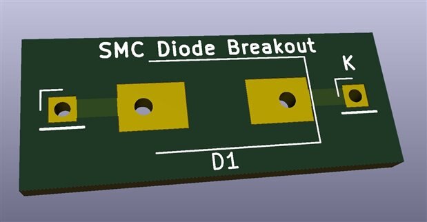
    I use KiCad and this would be a good starter project for it.  Out of curiosity I checked to see if it had the SMC footprint built in and it does.  In fact, it has a hand solder version which I had a look at.  There is a via through the footprint to a pad on the other side in their hand solder version which is interesting.  It would be easy to solder.  I encourage you to try building it yourself but let us know if you would like suggestions or feedback.

    image

    • Cancel
    • Vote Up +5 Vote Down
    • Sign in to reply
    • Verify Answer
    • Reject Answer
    • Cancel
  • Andrew J
    0 Andrew J over 7 years ago in reply to shabaz

    Thanks Shabaz.  I realise now I didn’t change the default copper thickness used in the calculator, which is 2oz, so I ended up with half the value that I should have.


    The pads in the data sheet are about half the width of those used above, enough area for the two tabs under the component which would make it difficult for hand soldering - I guess paste and a hot-air gun would be needed.  This conversation has given me a bit of insight in how to decide on, or adjust, footprints for SMD parts.  And to ensure I double check my calculations image  It does seem sometimes that there are so many things to get wrong!!


    Thanks


    Andrew

    • Cancel
    • Vote Up +2 Vote Down
    • Sign in to reply
    • Verify Answer
    • Cancel
  • shabaz
    0 shabaz over 7 years ago in reply to Andrew J

    Hi Andrew,


    I've not used KiCAD so I can't point to the specifics, but there will be a design rule check (DRC) tool in KiCAD, and running that will pick up things like traces too close to holes. It possibly might not pick up that trace that Frank highlighted in yellow, since that may not be violating any of its rules, even though it is not needed.

    There's a bit of extra resistance with the thin traces, so there would be a voltage drop if high current is passing, even if the traces can handle the slight rise in temperature, so you might prefer to thicken up some of them. That is impressive that you've done the schematic entry and PCB design with KiCAD as a first attempt.. I think it would electrically function.

    Regarding the diode land pattern/footprint, as Frank says, there will be a recommendation in the datasheet, so that can be a start. For nearly all SMD parts, I find the default recommendation to be acceptable for hand-soldering too, even though the datasheet land pattern is normally for an automated process (e.g. reflow or wave). As Frank says, optionally you could increase the size of the pad outward, to make it a bit easier if the pads don't already extend much beyond the component physical dimensions in the datasheet. Sometimes I may extend by 0.3mm or so, for certain components which have an overhang (e.g. large surface mount inductors with an outer ferrite shield that goes beyond the land pattern). For that diode package, that isn't the case, so the datasheet land pattern should be fine.


    I'm not sure why there are holes in the land pattern, I'm wondering if they are for optionally soldering a through-hole diode instead, i.e. the land pattern is dual-purpose maybe.

    Normally holes in pads are not used unless they are filled (i.e. commercial PCBs) since solder will drip through otherwise, but for home prototyping sometimes they are necessary (in which case I'll try to use the smallest hole possible). For a SMD diode breakout board, the holes shouldn't be needed in the pad I think, unless I'm missing something.

    • Cancel
    • Vote Up +3 Vote Down
    • Sign in to reply
    • Verify Answer
    • Reject Answer
    • Cancel
  • Andrew J
    0 Andrew J over 7 years ago in reply to fmilburn

    I'm sure I used that calculator and got .15mm!  I'll dig deeper into this, and Kicad, thanks for the heads up. 


    Thanks


    Andrew

    • Cancel
    • Vote Up +2 Vote Down
    • Sign in to reply
    • Verify Answer
    • Cancel
Reply
  • Andrew J
    0 Andrew J over 7 years ago in reply to fmilburn

    I'm sure I used that calculator and got .15mm!  I'll dig deeper into this, and Kicad, thanks for the heads up. 


    Thanks


    Andrew

    • Cancel
    • Vote Up +2 Vote Down
    • Sign in to reply
    • Verify Answer
    • Cancel
Children
No Data
element14 Community

element14 is the first online community specifically for engineers. Connect with your peers and get expert answers to your questions.

  • Members
  • Learn
  • Technologies
  • Challenges & Projects
  • Products
  • Store
  • About Us
  • Feedback & Support
  • FAQs
  • Terms of Use
  • Privacy Policy
  • Legal and Copyright Notices
  • Sitemap
  • Cookies

An Avnet Company © 2026 Premier Farnell Limited. All Rights Reserved.

Premier Farnell Ltd, registered in England and Wales (no 00876412), registered office: Farnell House, Forge Lane, Leeds LS12 2NE.

Follow element14

  • X
  • Facebook
  • linkedin
  • YouTube