element14 Community
element14 Community
    Register Log In
  • Site
  • Search
  • Log In Register
  • Community Hub
    Community Hub
    • What's New on element14
    • Feedback and Support
    • Benefits of Membership
    • Personal Blogs
    • Members Area
    • Achievement Levels
  • Learn
    Learn
    • Ask an Expert
    • eBooks
    • element14 presents
    • Learning Center
    • Tech Spotlight
    • STEM Academy
    • Webinars, Training and Events
    • Learning Groups
  • Technologies
    Technologies
    • 3D Printing
    • FPGA
    • Industrial Automation
    • Internet of Things
    • Power & Energy
    • Sensors
    • Technology Groups
  • Challenges & Projects
    Challenges & Projects
    • Design Challenges
    • element14 presents Projects
    • Project14
    • Arduino Projects
    • Raspberry Pi Projects
    • Project Groups
  • Products
    Products
    • Arduino
    • Avnet & Tria Boards Community
    • Dev Tools
    • Manufacturers
    • Multicomp Pro
    • Product Groups
    • Raspberry Pi
    • RoadTests & Reviews
  • About Us
    About the element14 Community
  • Store
    Store
    • Visit Your Store
    • Choose another store...
      • Europe
      •  Austria (German)
      •  Belgium (Dutch, French)
      •  Bulgaria (Bulgarian)
      •  Czech Republic (Czech)
      •  Denmark (Danish)
      •  Estonia (Estonian)
      •  Finland (Finnish)
      •  France (French)
      •  Germany (German)
      •  Hungary (Hungarian)
      •  Ireland
      •  Israel
      •  Italy (Italian)
      •  Latvia (Latvian)
      •  
      •  Lithuania (Lithuanian)
      •  Netherlands (Dutch)
      •  Norway (Norwegian)
      •  Poland (Polish)
      •  Portugal (Portuguese)
      •  Romania (Romanian)
      •  Russia (Russian)
      •  Slovakia (Slovak)
      •  Slovenia (Slovenian)
      •  Spain (Spanish)
      •  Sweden (Swedish)
      •  Switzerland(German, French)
      •  Turkey (Turkish)
      •  United Kingdom
      • Asia Pacific
      •  Australia
      •  China
      •  Hong Kong
      •  India
      •  Japan
      •  Korea (Korean)
      •  Malaysia
      •  New Zealand
      •  Philippines
      •  Singapore
      •  Taiwan
      •  Thailand (Thai)
      •  Vietnam
      • Americas
      •  Brazil (Portuguese)
      •  Canada
      •  Mexico (Spanish)
      •  United States
      Can't find the country/region you're looking for? Visit our export site or find a local distributor.
  • Translate
  • Profile
  • Settings
Community Hub
Community Hub
Member's Forum What’s the worst mistake/problem you’ve made during a project, and what did you learn from it? We are asking e14 in our Join, Share & Win Competition
  • Blog
  • Forum
  • Documents
  • Quiz
  • Events
  • Leaderboard
  • Polls
  • Files
  • Members
  • Mentions
  • Sub-Groups
  • Tags
  • More
  • Cancel
  • New
Join Community Hub to participate - click to join for free!
Actions
  • Share
  • More
  • Cancel
Forum Thread Details
  • Replies 59 replies
  • Subscribers 593 subscribers
  • Views 1645 views
  • Users 0 members are here
  • rasberrypi
  • win
  • aske14
Related

What’s the worst mistake/problem you’ve made during a project, and what did you learn from it? We are asking e14 in our Join, Share & Win Competition

E14Alice
E14Alice 18 days ago

Hello Everyone!

Hope you are all doing well. I’m excited to announce that this month's AskE14 question is: What is the worst mistake or problem you've encountered during a project, and what did you learn from it?

Sharing your experiences can help others identify similar challenges and understand how to overcome them. I hope this discussion will be beneficial for those who are just starting out on a project or feeling stuck with a problem.

Here's the question:

What’s the worst mistake/problem you’ve made during a project, and what did you learn from it? 

imageimage

Competition Details

You'll have to be a member of the element14 Community to join in and take part in this “Join, Share & Win” challenge. It's simple, all you have to do is:

1. You need to make sure you are Register  or Login
2. Then answer the following question by adding a reply or commenting!

What’s the worst mistake/problem you’ve made during a project, and what did you learn from it?  

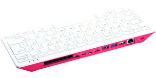
The Community team will then select the best 3 answers to win a Raspberry Pi 400!

This month, we are giving away:

image

Learn more

Terms and Conditions 

imagePDF

  • Sign in to reply
  • Cancel

Top Replies

  • dougw
    dougw 17 days ago +8
    My first rude awakening on the job was building a linear regulator to output 4A at 5V with a car battery as the input. I used a 2N3055 (TO3) as the pass transistor because it could handle 15 Amps and 115…
  • gordonmx
    gordonmx 17 days ago +6
    Many years ago, I worked for a company that made portable computers. A large service company wanted an add-on module base with more battery power to boost the operating life. The original computer had…
  • chloro
    chloro 17 days ago +5
    My worst project mistake? I guess I would say trusting a breadboard connection that “looked fine.” I spent hours debugging firmware, rewriting code, and questioning my life choices… only to find one…
Parents
  • ralphjy
    ralphjy 17 days ago

    Back in the early 80's when we were first learning to design 6 and 8 layer PCBs and we had limited ERC and DRC rules,  I made a critical current density error in a PCB design.  We were doing high power and high performance designs where we used power and ground planes for power distribution and impedance control.  I had a design that was using a coplanar waveguide for critical signal delivery.  I had instructed the PCB designer to stitch the coplanar and bottom ground planes together with closely spaced vias.  The waveguide worked great,  but because this was before the use of blind vias, I had inadvertently perforated a high power trace that ran below the bottom ground plane.  Our existing ERC/DRC checks passed.  Of course, the design powered up and checked out fine, but after several hours of operation - the board went up in flames.  It was extremely fortunate that I was there when it happened and was able pull the PCB from the backplane before the system caught fire.  

    After that I always made sure that I checked power and ground film for via perforation to identify and fix areas that would have high current density.  Years afterward we had a DFM group that helped check for these types of errors and many others that I hadn't considered.  I've had other less dramatic failures that were mitigated by DFM.  When we first started designing our own custom ICs, a hard lesson that we had to learn was to match the TCEs between the PCB and component substrates.  Not doing that caused reliability failures due to attachment failures.

    • Cancel
    • Vote Up +4 Vote Down
    • Sign in to reply
    • Cancel
Reply
  • ralphjy
    ralphjy 17 days ago

    Back in the early 80's when we were first learning to design 6 and 8 layer PCBs and we had limited ERC and DRC rules,  I made a critical current density error in a PCB design.  We were doing high power and high performance designs where we used power and ground planes for power distribution and impedance control.  I had a design that was using a coplanar waveguide for critical signal delivery.  I had instructed the PCB designer to stitch the coplanar and bottom ground planes together with closely spaced vias.  The waveguide worked great,  but because this was before the use of blind vias, I had inadvertently perforated a high power trace that ran below the bottom ground plane.  Our existing ERC/DRC checks passed.  Of course, the design powered up and checked out fine, but after several hours of operation - the board went up in flames.  It was extremely fortunate that I was there when it happened and was able pull the PCB from the backplane before the system caught fire.  

    After that I always made sure that I checked power and ground film for via perforation to identify and fix areas that would have high current density.  Years afterward we had a DFM group that helped check for these types of errors and many others that I hadn't considered.  I've had other less dramatic failures that were mitigated by DFM.  When we first started designing our own custom ICs, a hard lesson that we had to learn was to match the TCEs between the PCB and component substrates.  Not doing that caused reliability failures due to attachment failures.

    • Cancel
    • Vote Up +4 Vote Down
    • Sign in to reply
    • Cancel
Children
  • dang74
    dang74 17 days ago in reply to ralphjy

    It would be easy to make this kind of mistake in this day and age as well.  Thanks for sharing.

    • Cancel
    • Vote Up 0 Vote Down
    • Sign in to reply
    • Cancel
element14 Community

element14 is the first online community specifically for engineers. Connect with your peers and get expert answers to your questions.

  • Members
  • Learn
  • Technologies
  • Challenges & Projects
  • Products
  • Store
  • About Us
  • Feedback & Support
  • FAQs
  • Terms of Use
  • Privacy Policy
  • Legal and Copyright Notices
  • Sitemap
  • Cookies

An Avnet Company © 2026 Premier Farnell Limited. All Rights Reserved.

Premier Farnell Ltd, registered in England and Wales (no 00876412), registered office: Farnell House, Forge Lane, Leeds LS12 2NE.

ICP 备案号 10220084.

Follow element14

  • X
  • Facebook
  • linkedin
  • YouTube