element14 Community
element14 Community
    Register Log In
  • Site
  • Search
  • Log In Register
  • Community Hub
    Community Hub
    • What's New on element14
    • Feedback and Support
    • Benefits of Membership
    • Personal Blogs
    • Members Area
    • Achievement Levels
  • Learn
    Learn
    • Ask an Expert
    • eBooks
    • element14 presents
    • Learning Center
    • Tech Spotlight
    • STEM Academy
    • Webinars, Training and Events
    • Learning Groups
  • Technologies
    Technologies
    • 3D Printing
    • FPGA
    • Industrial Automation
    • Internet of Things
    • Power & Energy
    • Sensors
    • Technology Groups
  • Challenges & Projects
    Challenges & Projects
    • Design Challenges
    • element14 presents Projects
    • Project14
    • Arduino Projects
    • Raspberry Pi Projects
    • Project Groups
  • Products
    Products
    • Arduino
    • Avnet Boards Community
    • Dev Tools
    • Manufacturers
    • Multicomp Pro
    • Product Groups
    • Raspberry Pi
    • RoadTests & Reviews
  • Store
    Store
    • Visit Your Store
    • Choose another store...
      • Europe
      •  Austria (German)
      •  Belgium (Dutch, French)
      •  Bulgaria (Bulgarian)
      •  Czech Republic (Czech)
      •  Denmark (Danish)
      •  Estonia (Estonian)
      •  Finland (Finnish)
      •  France (French)
      •  Germany (German)
      •  Hungary (Hungarian)
      •  Ireland
      •  Israel
      •  Italy (Italian)
      •  Latvia (Latvian)
      •  
      •  Lithuania (Lithuanian)
      •  Netherlands (Dutch)
      •  Norway (Norwegian)
      •  Poland (Polish)
      •  Portugal (Portuguese)
      •  Romania (Romanian)
      •  Russia (Russian)
      •  Slovakia (Slovak)
      •  Slovenia (Slovenian)
      •  Spain (Spanish)
      •  Sweden (Swedish)
      •  Switzerland(German, French)
      •  Turkey (Turkish)
      •  United Kingdom
      • Asia Pacific
      •  Australia
      •  China
      •  Hong Kong
      •  India
      •  Korea (Korean)
      •  Malaysia
      •  New Zealand
      •  Philippines
      •  Singapore
      •  Taiwan
      •  Thailand (Thai)
      • Americas
      •  Brazil (Portuguese)
      •  Canada
      •  Mexico (Spanish)
      •  United States
      Can't find the country/region you're looking for? Visit our export site or find a local distributor.
  • Translate
  • Profile
  • Settings
Community Hub
Community Hub
Member's Forum What beginners mistakes have I made?
  • Blog
  • Forum
  • Documents
  • Quiz
  • Events
  • Leaderboard
  • Polls
  • Files
  • Members
  • Mentions
  • Sub-Groups
  • Tags
  • More
  • Cancel
  • New
Join Community Hub to participate - click to join for free!
Actions
  • Share
  • More
  • Cancel
Forum Thread Details
  • Replies 20 replies
  • Subscribers 510 subscribers
  • Views 1013 views
  • Users 0 members are here
Related

What beginners mistakes have I made?

mpiechotka
mpiechotka over 7 years ago

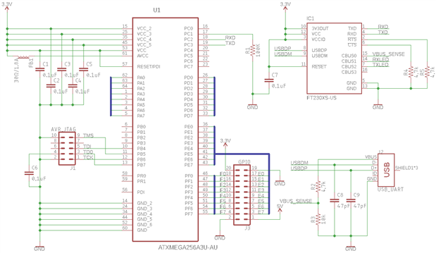
Sorry if this is incorrect forum/basic question. While I have a background in programming and some experience with FPGAs the I didn't know much about EE before. I run into a hobby project for which I'd like to create a PCB and soon I found myself in deep waters. So I decided to step back and create a simple PCB to learn basics. I tried to create a simple AVR board with an GPIO header, JTAG connector and USB-to-UART bridge. I've created something but I'm sure I've done many basic mistakes and strange decisions so I'd be grateful for pointing them out.


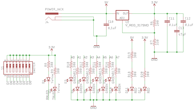
PS. I know there is no power switch but I couldn't find one on with eagle library.

image

image

image

  • Sign in to reply
  • Cancel

Top Replies

  • michaelkellett
    michaelkellett over 7 years ago +6
    Things you might consider: 1) use a ground plane on the lower (non component side) of the baord. 2) keep all the components on one side (if you will hand solder a couple of prototypes this doesn't matter…
  • genebren
    genebren over 7 years ago +3
    Not sure how important this is, but the FT230X documentation calls for 27 ohm resistors inline on on the D+ and D- lines. Also, I am not sure that on the FT230X, that the VCC pin should be tied to the…
  • shabaz
    shabaz over 7 years ago in reply to mpiechotka +3
    Hi Maciej, Its easiest if you can find some example physical PCBs, and examine them closely, to see patterns to follow. Here is an example. Position 1 is a pad belonging to an IC. You can see that the…
  • michaelkellett
    michaelkellett over 7 years ago

    Things you might consider:


    1) use a ground plane on the lower (non component side) of the baord.

    2) keep all the components on one side (if you will hand solder a couple of prototypes this doesn't matter but for production it always costs more to populate both sides.)

    3) don't ever make sharp V shapes with track - it causes problems in etching

    4) try to take tracks out of sm components on axis and the same for all

    5) you have some very thin tracks and some tiny vias - you don't need to use such aggressive design rules a board like this.


    MK

    • Cancel
    • Vote Up +6 Vote Down
    • Sign in to reply
    • Cancel
  • eagleenthusiast
    eagleenthusiast over 7 years ago in reply to michaelkellett

    Michael,


    I agree with all of your statements. Can you explain better your #4 advice?

    • Cancel
    • Vote Up 0 Vote Down
    • Sign in to reply
    • Cancel
  • shabaz
    shabaz over 7 years ago in reply to eagleenthusiast

    Hi S D,


    Basically it means that whatever the orientation of the component (typically they are at zero or 90 degrees orientation to each other and the board edges), then ideally the traces out of the pads of the component should be placed at these angles too, i.e. if you start at the pad of a component, then preferably the trace from it should be routed at zero or 90 degrees too, and not at some other angle. Once the trace is a distance away from the component pad, then it can be routed at a different angle if desired.

    • Cancel
    • Vote Up +1 Vote Down
    • Sign in to reply
    • Cancel
  • genebren
    genebren over 7 years ago

    Not sure how important this is, but the FT230X documentation calls for 27 ohm resistors inline on on the D+ and D- lines.  Also, I am not sure that on the FT230X, that the VCC pin should be tied to the VCCIO and 3V3OUT pins.  Power should be connected to VCC (with a 0.1uF bypass cap to ground) and VCCIO, RESET and 3V3OUT should be connected together with another 0.1uF cap to ground.  I would also add a diode between the power jack and the regulator for reverse power protection.


    Good luck with your project!

    Gene

    • Cancel
    • Vote Up +3 Vote Down
    • Sign in to reply
    • Cancel
  • michaelkellett
    michaelkellett over 7 years ago in reply to shabaz

    Thanks Shabaz,


    I'm wrestling with a switch chip that doesn't want to talk to an FPGA so a bit pushed for time today.


    MK

    • Cancel
    • Vote Up +2 Vote Down
    • Sign in to reply
    • Cancel
  • mpiechotka
    mpiechotka over 7 years ago in reply to michaelkellett

    Thanks Michael


    AD 3. Thanks - I haven't realized that one - the explanations I read was about current flow which is why I tried to kept angles for flow <45°.


    AD 4. Sorry - I have no clue what you mean.


    AD 5. I use default 6 mils for signals and for power/ground signals that supply a lot of components I choose 20. I'm not sure what to choose if default are not correct - obviously the thinner the track the less conductivity it has and I know I could calculate in principle the resistance but probably there are some good rules of thumb.

    • Cancel
    • Vote Up +1 Vote Down
    • Sign in to reply
    • Cancel
  • dougw
    dougw over 7 years ago in reply to mpiechotka

    It might be worth increasing the trace width to the power pins on the USB connector...

    • Cancel
    • Vote Up +2 Vote Down
    • Sign in to reply
    • Cancel
  • luislabmo
    luislabmo over 7 years ago in reply to michaelkellett

    Do you care to elaborate on #1? why no GND plane on the components side of the board ?


    Luis

    • Cancel
    • Vote Up +1 Vote Down
    • Sign in to reply
    • Cancel
  • shabaz
    shabaz over 7 years ago in reply to mpiechotka

    Hi Maciej,


    Its easiest if you can find some example physical PCBs, and examine them closely, to see patterns to follow.

    Here is an example.

    Position 1 is a pad belonging to an IC. You can see that the trace marked 2 comes off at a nice angle (zero degrees) before it bends at position 3.

    Similarly, look at the pad marked 4. This belongs to a surface mount resistor or capacitor. Again, the trace comes off at a nice angle (zero degrees) before it gets bent near position 5, and then disappears off into a via shown in green.


    Similarly, position 6 shows a capacitor. Here the trace comes off at 90 degrees before it bends at any other angle.

    Now look to position 7. This is a through-hole pad for a dual-in-line header, like you are using in your design. Here there was not enough room to easily come off at zero or 90 degrees, so 45 degrees was used, but exactly through the centre of the pad, as if the pad were a clock face, and the trace was one of the clock hands, starting at the centre of the pad. In other words, don't bring a trace to a through-hole pad in a way that the trace and pad together look like a music note (or golf club) shape combined.


    Also, 6 mil is unnecessary for your design. The example PCB below is more dense than yours, and all the visible traces are nearly all 10mil (with a few that are 8mil, you can just about see the difference widths if you look closely). There are no 6mil traces here.

    image

    • Cancel
    • Vote Up +3 Vote Down
    • Sign in to reply
    • Cancel
  • genebren
    genebren over 7 years ago in reply to shabaz

    I would also add that the example added by shabaz shows some very good examples of spacing between traces.  When possible, leave ample spacing between traces as this reduces potential interference between signals.  In your design, near the GPIO connector and also the JTAG connector, a lot traces bunch up together.  You could move each trace further from the others and produce a clearer (aesthetically and electronically) board.  Layout is sort of an art and a science, mixed together.


    Gene

    • Cancel
    • Vote Up +1 Vote Down
    • Sign in to reply
    • Cancel
>
element14 Community

element14 is the first online community specifically for engineers. Connect with your peers and get expert answers to your questions.

  • Members
  • Learn
  • Technologies
  • Challenges & Projects
  • Products
  • Store
  • About Us
  • Feedback & Support
  • FAQs
  • Terms of Use
  • Privacy Policy
  • Legal and Copyright Notices
  • Sitemap
  • Cookies

An Avnet Company © 2025 Premier Farnell Limited. All Rights Reserved.

Premier Farnell Ltd, registered in England and Wales (no 00876412), registered office: Farnell House, Forge Lane, Leeds LS12 2NE.

ICP 备案号 10220084.

Follow element14

  • X
  • Facebook
  • linkedin
  • YouTube