


Introduction
This is a follow-up to A Transistor Load which I blogged about as part of the Project14 Test and Instrumentation competition.
Since then I've been looking at the way the load performs, so this blog is on the subject of stability. By 'stability', I mean not only whether there's the
possibility of the circuit breaking into sustained oscillations, but whether we might be close to that and the waveforms might
ring badly (damped oscillations). To do this, I'm going to use the simulator to open the loop (I don't have good enough test
equipment to do that for real with the physical circuit, there the best I can manage is to look at the closed-loop waveforms
on an oscilloscope). The simulator won't model the circuit totally accurately, but it does give me the basics of what is going
on and any compensation I come up with in the simulator should be applicable to the real circuit with a bit of tweeking of
values.
When I designed the load, I originally hoped that it would be really fast and have the kind of performance to outdo an op amp
approach (at least, one designed with low-cost, internally-compensated op amps) but, alas, that wasn't to be and it's probably
only just comparable. The major problem with instability comes from the same root as with any load, not the basic amplifier
driving the control loop but any external inductance in the output loop (which, unless we're being silly and trying to drive
actual inductors, means the connection leads) and its interaction with the feedback loop, but I'm getting ahead of myself -
more on that later.
Open Loop Analysis in the Simulator
The simulator I'm using here is the free one from Texas Instruments. Other SPICE simulators would do equally well.
Here is the circuit as I simulated it. This has a few minor corrections compared to the original one, the main one being that
I noticed that the preset potentiometers, which I thought were 10 ohms, are actually 100 ohms. (A value of 100 ohms suits the
zero pot better than the 10 but with the other one I put a 10 ohm resistor across it to reduce the range.)

To open the loop and generate Bode plots, I've inserted a silly value of inductance (1TH - yes, that really is one tera Henry,
ie one thousand billion Henries) and a silly value of capacitance (1TF - one tera Farad) between the sense point at the top of
the current-sense resistor and the resistor network that feeds the voltage back. The generator drives the feedback and the
meter that measures the output is connected across the sense resistor (where the voltage is equivalent to the current
flowing). The point of the silly-value components is that at dc the loop is closed and the generator is disconnected, so the
simulator can determine the correct dc operating points, and for ac the loop is open and is driven as though it were a
straight amplifier, without any feedback, so we can measure the response. I could have opened the loop anywhere around the
overall feedback loop and the results should be broadly the same [that presumes a linear system, so that superposition applies
- that isn't the case with transistors and the MOSFET for large signals, but is a good approximation with the very small
signals used by the simulator's transfer function], but there is a possible issue with impedance matching to the generator to
be aware of (the zero ohm output impedance of the generator roughly matches how the output MOSFET and the current-sense
resistor drive the feedback resistors).
Basic Compensation
As you can see from the circuit, I'm starting with the output lead inductance (L2) being zero (so it's like a perfect
connection wire) and the compensation capacitor (C1) also being zero (effectively, not there). I find that it's quicker just
to set these to zero when they're not wanted rather than to take them out of circuit and then have to re-introduce them. Here
are the Bode plots (unfortunately, the software can't always make up its mind how to present the phase scale on the left - so
on the later ones you'll see a scale from +180 to -180, which is equivalent to what you see here):

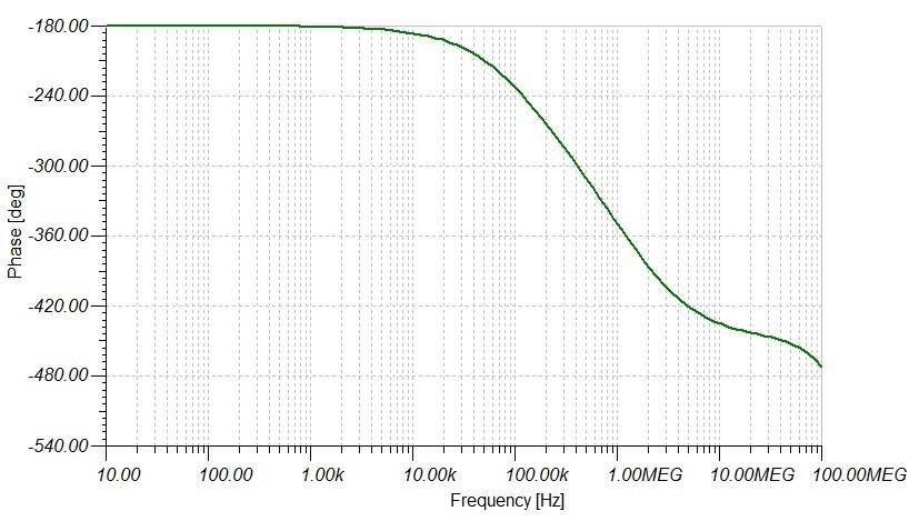
Is this going to be stable? Well, I already know the answer to that because when I first built the load I left out the
capacitor and this was the result,

but can we tell that from the Bode plots?
Yes, we can. If we look at the phase curve, we can see that the curve crosses -360 degrees at around 1.2MHz. At that
frequency, the magnitude curve shows 14.5dB of gain (that's only a gain of 5.3, but anything over one will allow an
oscillation to build), so the conditions are there for oscillation. There is another way we can tell because the magnitude
curve and the phase curve aren't actually independent and there is a relationship between the two, so the fact that the curve
is so steep as it passes through the 0dB level would tell an experienced designer that there's a problem, even without having
the phase curve to look at.
If I simulate it closed-loop with the same triangle waveform at the input as I had when I tested it, this is the resulting
waveform
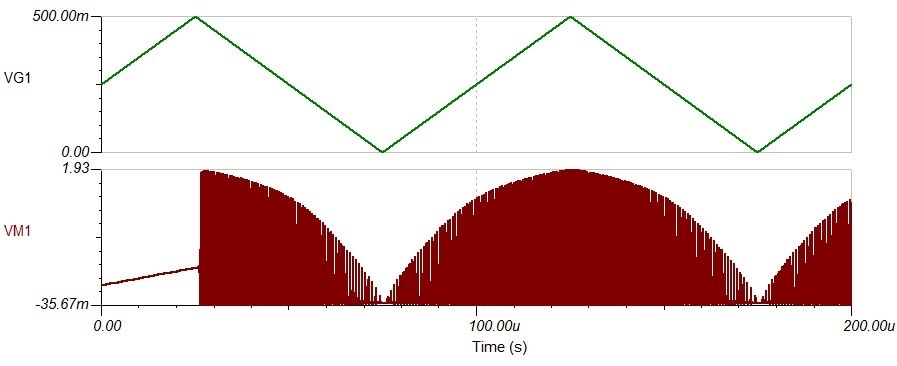
That's more extreme than the real circuit, a useful reminder that the real circuit has parasitic capacitances that affect the
results somewhat [it's hard to achieve a 0pF capacitance on an open circuit board, for instance]. As a slight aside, something
that's interesting with that plot is that the simulated oscillation doesn't take off until the waveform reaches the peak where
the sudden change in direction introduces frequency components of an appropriate frequency to start the oscillation. That's
because my simulation is perfectly quiet and doesn't have the low-level noise that any real circuit would have - the real
circuit just spontaneously bursts into oscillation, it doesn't need to be kicked.
Before I go further, perhaps I should mention where that steep slope that gives us the problem comes from. Whilst transistors
are surprisingly well behaved, towards the top end of their frequency range intrinsic capacitance causes the gain to roll off.
It's that capacitance that gives the problem. With several devices it soon adds up to enough delay in the signal that it's
effectively inverted and our negative feedback changes to positive feedback. The real situation is more confused than the
simulator shows because in a real circuit the devices would all be slightly different, whereas here all the 2N3904 transistors
have exactly the same characteristics.
So how do we do something to stop the oscillation? Basically, we need to shape the frequency response so that when the
magnitude curve passes through 0dB the slope is below the level where the corresponding phase shift would give us problems. We
can do that with a frequency-dependent network of some sort (usually made up of capacitors and resistors). We are looking here
at the response around the whole loop, so that suggests we can place that network either in the forward path through the
amplifier or in the feedback, and there's also nothing to stop us having more than one shaping network if that's useful to us.
One classic and very simple way to achive compensation that has been used a very great deal over the years is to include a
capacitor acting as an integrator. There are some disadvantages with the approach but it does make for a very stable system.
One reason for its popularity is that if you place it round a transistor, on an integrated circuit, the effective capacitor
value is the actual value multiplied by the gain (look up Millar effect if you're interested). That was useful to IC designers
because on-chip capacitors take up considerable space, even for modest values of capacitance, and the smaller they can get
them the better.
The capacitor I've placed at C1 works as an integrator, though in this case I've taken it to the gate drive rather than just
place it from base to collector on the input transistor (T3). It then includes all the active transistors in the loop other
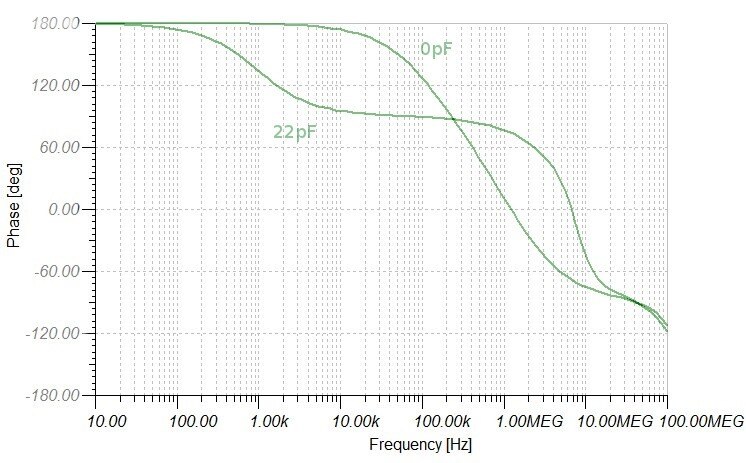
than the MOSFET. These next two plots show the situation for magnitude and phase response with no capacitor and a 22pF
capacitor.
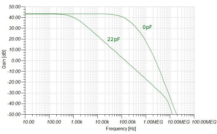
Looking at the magnitude plot first, it's evident that the slope with the 22pF is now much shallower as it comes down. That's
because it's dominated by the effect of the integrator capacitor where the response changes at 20dB per decade (6db/octave). A
name for this kind of compensation is "dominant pole". That's because the additional pole introduced by the capacitor has been
positioned low down in frequency, far below those coming from the intrinsic capacitances of the transistors, and so it then
dominates the response and removes the gain before we get up to the area where that cluster of awkward poles will give us
problems. If we move to the phase plot, we can see the advantageous effect of using an integrator. When the phase moves away
from the 180 value that we get at low frequencies, it shifts by 90 degrees and then sits there over a considerable range of
frequencies (that's what an integrator does - think of it as integrating a sinewave giving you a cosine). That's good because
it keeps the phase well away from the 0 degree line and gives close to 90 degrees of phase margin (the margin is the
difference between 0 degrees and the curve value at any frequency where the gain is more than 0dB). We can also see that it
doesn't fall to 0 degrees [the point where you WILL get oscillation IF there's the gain to support it] until the curve is up
to around 7MHz. At that frequency, the gain has fallen much further and is around -35dB, so that gives us a good gain margin.
Both values are very safe and ensure that, whatever we throw at it, it isn't going to spontaneously break into oscillation.
Dynamic Response
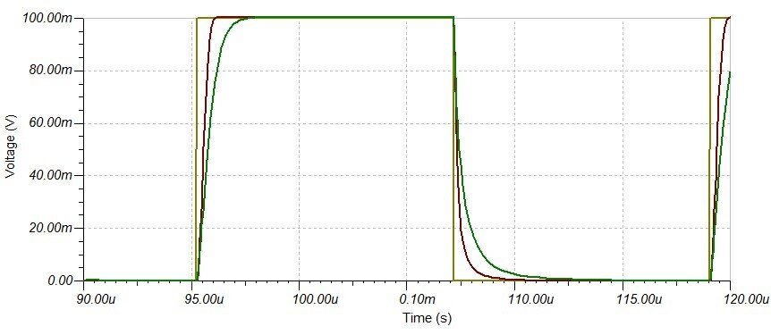
One factor that we need to keep in mind with this focus on stability is that there are other considerations. If I do a
transient plot for 11pF and 22pF, both of which are stable in the simulator (the simulator shows we only need greater than
3pF), then we get this. The red trace is the output with 11pF, the green trace is the output with 22pF, and the amber trace is
the input signal which the output is trying to follow. For a large signal step, the compensation affects the dynamic response.
The 11pF looks like it's critically damped, the 22pF is slower and slightly over-damped.
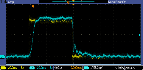
That all looks nice and clean in the simulator. On the bench it's much more messy. Here's the trace for 11pF
And here's the trace for 22pF
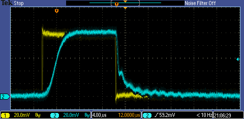
They are both much less well behaved. It's also noticeable that the behaviour as we come down towards 0A on the output is far
less assured than the step up to 1A.
Effect of Lead Inductance
In this section I'm going to look at the effect of lead inductance on the load. We would like our connection leads not to act
like inductors but, as soon as we pass a current through them, a magnetic field will develop and so they will act like one
whether we want them to or not. The inductance is low, a metre of typical hook-up wire will have an inductance of something
like xxxx, and in many situations it doesn't matter or can even be advantageous. But, in the situation of this particular
active load that I've designed, it turns out to be a real nuisance and affects the operation in a very significant way.
For simplicity in the simulation, I've lumped both leads together into a single inductor connected to the drain of the MOSFET,
but take that as being the sum of both leads used to connect the external supply (I think it's valid to do that).
Here are the results as I vary that inductor with values of 0nH, 100nH, 200nH, 400nH, and 800nH.
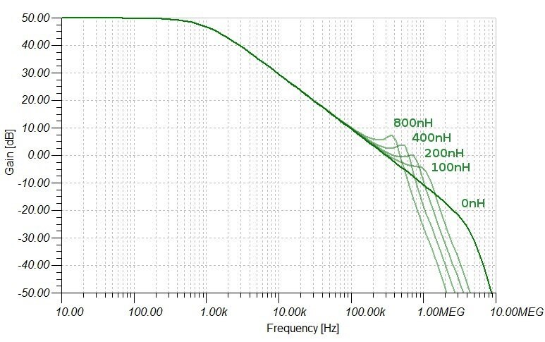

[I don't understand the step change on the phase curves. It looks like it is some kind of artefact that occurs when the gain drops to a very low value.]
The diagrams show clearly the effect of increasing the inductance. From the magnitude curve, we can see that with any more
than 200nH of inductance the curve is steep enough as it crosses 0dB to cause actual oscillation. For these cases, the point
where the phase curves cross the 0 degrees line gives the approximate frequency of oscillation (very approximate because not
only is this a very imperfect model, missing parasitics present in the build, but there is also natural variation between the
components that isn't being taken into account). Below 200nH the situation is still fraught, with a gain margin of only 5dB
for the 100nH curve (which would cause the output to ring very badly if subjected to step change).
So the situation I'm in is that though it was easy to compensate the basic voltage amplifier made up of the bipolar
transistors to ensure good stability, with the addition of even just very modest amounts of inductance in the output circuit
that's completely wrecked.
Further Work
This is still very much a work in progress. So where do I go from here? I need to see if I can find a way to compensate the
whole system in such a way as to counter the effects of the inductance. One obvious way would be to increase the value of the
compensation capacitor - as the compensation slope moves to the left, the distruption from the inductance falls lower and
lower on the magnitude curve until the whole thing is nicely stable and there's a good gain margin - but a side effect is that
it massively restricts the closed-loop bandwidth. So I need to investigate more complex compensation schemes than single
dominant pole to see if I can retain a fair proportion of the bandwidth that the system currently has whilst getting it
solidly stable. That's going to mean more reading and experimenting.
There are two further problems with all this which I've glossed over here but are actually very important in the context of
the load. One is that I'm looking at small-signal stability - how the loop behaves for a very small signal - mainly because
that's the way the simulator calculates the response. But there is also the large signal response to consider. A disadvantage
of the integrator approach to compensation is that it takes time to charge and discharge the capacitor and that then places a
limit on the rate at which the output will move (the slew rate). You might think that there's also the gate-resistor/gate-
drain-capacitance of the MOSFET to consider, but the low-pass filter that that gives us is higher up than the 22pF
compensation roll-off so doesn't really play a part (I was a little surprised by that because I initially assumed it would
play a factorr and complicate things). The other problem that became evident in the course of doing all this is that the
compensation behaves differently at different input levels. If all the elements of the open loop were linear (which is what
texts seem to mostly presume) there wouldn't be any difference, but they aren't totally linear and that's particularly the
case with the MOSFET when we are down around the threshold voltage. That's enough of a problem that I've been toying with
ideas of biasing the MOSFET with a standing current (however that might be done) so that it never actually has to totally turn
off to get a zero current in the load output circuit loop. I also need to identify what it is that the inductance is
interacting with (the peakiness in the magnitude curve points to resonance between the inductance and a capacitor - presumably
the intrinsic drain capacitance of the MOSFET, though I'm not entirely sure because there are other possibilities). If I
understood that better it might point to other approaches to the problem (such as trying to hide the capacitance from the
inductance).
Any questions, feel free to ask - I won't necessarily be able to come up with an answer, but if not maybe others will.
Hopefully I haven't got too much of that wrong, but if you spot any errors or know that I'm wrong with any of the
explanations, please say.
Top Comments