element14 Community
element14 Community
    Register Log In
  • Site
  • Search
  • Log In Register
  • Community Hub
    Community Hub
    • What's New on element14
    • Feedback and Support
    • Benefits of Membership
    • Personal Blogs
    • Members Area
    • Achievement Levels
  • Learn
    Learn
    • Ask an Expert
    • eBooks
    • element14 presents
    • Learning Center
    • Tech Spotlight
    • STEM Academy
    • Webinars, Training and Events
    • Learning Groups
  • Technologies
    Technologies
    • 3D Printing
    • FPGA
    • Industrial Automation
    • Internet of Things
    • Power & Energy
    • Sensors
    • Technology Groups
  • Challenges & Projects
    Challenges & Projects
    • Design Challenges
    • element14 presents Projects
    • Project14
    • Arduino Projects
    • Raspberry Pi Projects
    • Project Groups
  • Products
    Products
    • Arduino
    • Avnet & Tria Boards Community
    • Dev Tools
    • Manufacturers
    • Multicomp Pro
    • Product Groups
    • Raspberry Pi
    • RoadTests & Reviews
  • About Us
  • Store
    Store
    • Visit Your Store
    • Choose another store...
      • Europe
      •  Austria (German)
      •  Belgium (Dutch, French)
      •  Bulgaria (Bulgarian)
      •  Czech Republic (Czech)
      •  Denmark (Danish)
      •  Estonia (Estonian)
      •  Finland (Finnish)
      •  France (French)
      •  Germany (German)
      •  Hungary (Hungarian)
      •  Ireland
      •  Israel
      •  Italy (Italian)
      •  Latvia (Latvian)
      •  
      •  Lithuania (Lithuanian)
      •  Netherlands (Dutch)
      •  Norway (Norwegian)
      •  Poland (Polish)
      •  Portugal (Portuguese)
      •  Romania (Romanian)
      •  Russia (Russian)
      •  Slovakia (Slovak)
      •  Slovenia (Slovenian)
      •  Spain (Spanish)
      •  Sweden (Swedish)
      •  Switzerland(German, French)
      •  Turkey (Turkish)
      •  United Kingdom
      • Asia Pacific
      •  Australia
      •  China
      •  Hong Kong
      •  India
      • Japan
      •  Korea (Korean)
      •  Malaysia
      •  New Zealand
      •  Philippines
      •  Singapore
      •  Taiwan
      •  Thailand (Thai)
      • Vietnam
      • Americas
      •  Brazil (Portuguese)
      •  Canada
      •  Mexico (Spanish)
      •  United States
      Can't find the country/region you're looking for? Visit our export site or find a local distributor.
  • Translate
  • Profile
  • Settings
Personal Blogs
  • Community Hub
  • More
Personal Blogs
Legacy Personal Blogs A Transistor Load: Stability Part 2
  • Blog
  • Documents
  • Mentions
  • Sub-Groups
  • Tags
  • More
  • Cancel
  • New
  • Share
  • More
  • Cancel
Group Actions
  • Group RSS
  • More
  • Cancel
Engagement
  • Author Author: jc2048
  • Date Created: 30 Dec 2018 12:13 AM Date Created
  • Views 802 views
  • Likes 6 likes
  • Comments 0 comments
  • linear design
  • analog design
  • negative feedback
  • circuit design
  • active load
  • feedback
  • nfb
  • transistors
  • jc2048
  • constant current load
Related
Recommended

A Transistor Load: Stability Part 2

jc2048
jc2048
30 Dec 2018

Introduction


This is a short follow-up to A Transistor Load

which I blogged about as part of the Project14 Test and Instrumentation competition.


In the last blog A Transistor Load: Stability

I got as far as compensating the amplifier section with a single 'dominant pole' capacitor and looking

at the way the dynamic response was affected by different capacitor values. I also looked at the issue of lead inductance

in the output current loop. I've done a little bit more work on it since then but it's all rather piecemeal and bitty and

that makes it difficult to blog about, so this is an update rather than a full blog.


Is 'Dominant Pole' Compensation the only Way to Ensure Stability?


In the last blog, I used a capacitor around the amplifier for the compensation. That capacitor turns the amplifier

section of the circuit into an integrator over a wide range of the bandwidth and the result is that the phase of the

open-loop amplifier is forced to a well-defined 90 degrees giving a good phase margin as the gain comes down to unity.

I've been experimenting with the simulator, but my optimism about being able to find an alternative hasn't come to much.


The fundamental problem is that to ensure stability we have to get the gain down well below unity by the time we get up

to the kind of frequencies where all the awkward poles will give us trouble. But at the same time, the rate at which the

gain lowers as we approach that unity point can't be too steep or the phase will get to 0 degrees whilst there is some

gain. That seems to be a circle that is difficult to square.


More On Lead Inductance


When I did the last blog, I looked at how lead inductance affected the stability. One thing that was evident was that the

inductance can see some capacitance that it will resonate with. Unfortunately for me, that resonance comes just where I

don't want it and with only fairly modest values of lead inductance (frequency-wise it pushes the gain around just above

the area where the open-loop gain gets down to unity). I wasn't clear what that capacitance was though I speculated that

it was one of the intrinsic capacitances in the MOSFET.


Since then I've discovered something that gives me some more clues. The behaviour with a drain voltage of 12V is very

different to how it behaves with a drain voltage of 3V. These next two traces show the two conditions - the top one is

12V and the bottom one 3V. I've set the input so that it moves the output between 1A and 3A to get away from my other

major problem that the load behaves much differently down at low output currents.


image


image


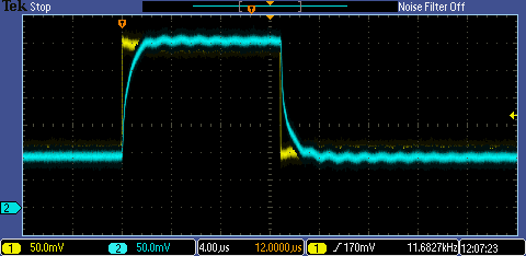
All conditions are the same for both traces except for the drain voltage.


At 12V, where the drain voltage is above the gate voltage, there is a small amount of residual ringing that takes a long

time to die away (not much damping). A simulation doesn't show that ripple, so its coming from something that doesn't get

modelled. At 3V, where the drain is below the gate voltage, there's very definite ringing which dies away more quickly.

That does show up in a simulation.


Here's what a simulation shows for the two cases, again 12V top and 3V beneath. These are for a lead inductance of 75nH.


image

image


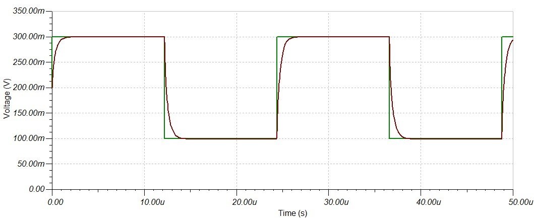
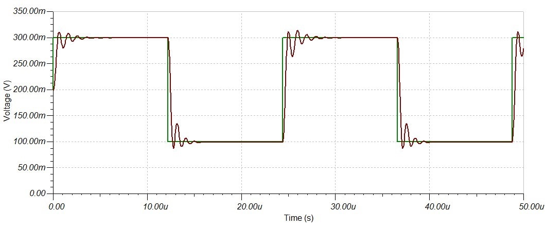
These are the curves that the datasheet gives, but these are for the condition where Vgs is 0V, not with current flowing

through the channel. I thought that I might have picked a particularly bad MOSFET for this, but comparison with

datasheets for similar devices shows that it is actually quite reasonable.


image


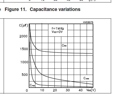
That shows the way the output capacitance of the MOSFET increases as the drain voltage comes below the threshold voltage and which is

presumably the root of most of my problems.


Further work


I've come up with a new version of the design, which seems to deal better with the lead inductance, so

the next thing on the agenda is to build it and see how far short of the promise it falls.

  • Sign in to reply
element14 Community

element14 is the first online community specifically for engineers. Connect with your peers and get expert answers to your questions.

  • Members
  • Learn
  • Technologies
  • Challenges & Projects
  • Products
  • Store
  • About Us
  • Feedback & Support
  • FAQs
  • Terms of Use
  • Privacy Policy
  • Legal and Copyright Notices
  • Sitemap
  • Cookies

An Avnet Company © 2025 Premier Farnell Limited. All Rights Reserved.

Premier Farnell Ltd, registered in England and Wales (no 00876412), registered office: Farnell House, Forge Lane, Leeds LS12 2NE.

ICP 备案号 10220084.

Follow element14

  • X
  • Facebook
  • linkedin
  • YouTube