


This one came out of reading about GaN FETs in this 'essentials' blog: Semiconductors I GaNFETs for Power Conversion
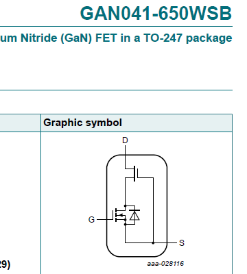
When I had a look at the datasheet for one of the parts being advertised, I realised from the
equivalent circuit that it was a cascode combination of an Si [silicon] MOSFET and a GaN [gallium
nitride] FET (it would appear that that combination has become available because it looks like they
are growing the GaN on a Si substrate). This is how it's shown in the datasheet:
Although I've come across the cascode configuration as a two-stage analogue amplifier, I'm not very
familiar with how it behaves when switching, so I thought I'd experiment a bit. The actual parts in
that article are very expensive [about £10 in one-off quantities], would have the disadvantage of my
not being able to probe the junction between the Si part and the GaN part anyway, and I don't have
good test equipment for working at high currents, so I've thrown together a very low-powered version
to look at.
My cascode uses a BS170 mosfet for the lower switch and a BF256BBF256B n-type JFET for the upper. This will
behave quite differently to the GaN FET, so don't treat the two as in any way equivalent, but it
enables me to get an idea how the switching occurs and what the pros and cons of such a configuration
might be.
I'm going to set up two switches side by side, one consisting of just a BS170 part and the other
being the cascode connected BS170 and BF256BBF256B. That way I can compare the two. The input is going to
come from an IO pin of an Arduino Uno. I've previously found that that makes quite a nice pulse
generator for this kind of experiment: the output pins are fast and well behaved.
Here's my circuit. I used a 2N7000, instead of the BS170, for the simulation because of difficulties
with importing a model for the BS170. They're very similar, though, in the way they behave.

Because the Idss [current when Vgs is zero] of the BF256BBF256B is only about 9mA, I'm going to need to
keep the load current a good bit below that, so my load is a 10k resistor. With the rail at 20V, that
will give a current of around 2mA when the switch is on, which is well within the capability of the
JFET to deal with.
Here's how the two outputs behave when they're switching [blue is the single MOSFET, yellow is the
cascode]

Here's how it looks in the simulator:

Although there are some minor differences [which we'd expect, as the actual devices won't perfectly
match the typical figures used for the models], the essential features of the waveforms are all
there, so the simulator is modelling the active devices reasonably well.
Here are the waveforms for switching on and switching off in more detail


The single device is faster to switch on, but seems to be slower to switch off. Something to notice
in that second waveform is that both curves are more or less the same up to 2.5V, where they then
start to diverge. To see better what was happening, I probed the cascode, with one probe on the drain
of the MOSFET [blue] and the other on the drain of the JFET [yellow].

Here's the turn off in more detail

It's not too difficult to work out what's happening here.
About two divisions across, the gate voltage falls and the turning off starts. Initially, the drain
of the MOSFET goes the wrong way. That's because the load is very light and the intrinsic capacitance
from the gate of the MOSFET to the drain can couple the very fast falling gate edge across. Once
that's out of the way, we see the MOSFET turning off and the voltage at the drain rising. The two
curves track each other because the JFET is still on at this point [the small difference between them
being the drop from the JFET's 'on' resistance]. As the voltage at the source of the JFET rises, the
gate held at zero volts is going negative with respect to it and the JFET will also start to turn
off. The two curves will then steadily diverge as the resistance of the JFET increases.
The voltage at the drain of the MOSFET then hovers at something like the inverse of the gate
threshold of the JFET. With both devices off, that node is isolated and the voltage is held by the
intrinsic capacitance within both parts. In reality, with the oscilloscope probe attached [10M
resistance], it will be a little lower as the probe will have the effect of discharging the
capacitance, resulting in the JFET then turning on slightly to counterbalance the discharge current.
Once both devices are fully off, the rest of the curve is then simply the 10k resistor charging the
capacitance at the drain of the JFET up to the rail voltage.
Looking at the cascode at the point where the transistors turn on we have this

Here we can see that the MOSFET is quite snappy, completing in about 10ns. Again, as with the turn
off, there's feedthrough of the gate signal to the drain.
In contrast the JFET seems slow. But that's because, although it is on, it regulates the current and
that results in this steady downward ramp of the voltage as it discharges the intrinsic capacitance
at the drain [plus the capacitance at the probe tip, of course].
So some tentative observations.
1. We can see that the MOSFET's drain voltage excursion with the cascode is low, even where the load
is tied to a high voltage rail. The top transistor is shielding the lower one from the voltage. In my
circuit that's irrelevant because both transistors happen to have the same 60V maximum drain voltage,
but with the GaN FET it means the lower Si part can be a low voltage one and I assume that means that
it can be made with lower intrinsic capacitances and so switch faster [for a given current].
2. A second advantage of the cascode is that the drain voltage doesn't have to move very far, so that
too speeds the switching time of the part. Presumably, that evens things up a bit between the Si part
and the GaN part: the GaN devive will be faster, but has the burden of slewing its output over a much
greater voltage.
3. Once both transistors are off, the cascode arrangement may have an advantage of less capacitance
at the output, but that's very dependent on device properties. In a sense, for the cascode, the top
transistor is shielding the load from the capacitance of the bottom transistor, but whether that
makes any real difference is a 'that depends' type question.
The circuit I'm experimenting with here isn't particularly useful with these small-current
components. There is, though, one thing I could try with it. As the bottom transistor stays in the 0
-5V range, instead of having a separate discrete transistor I could just substitute the one that's
inside the processor driving the I/O pin. Also, since the JFET will regulate the current to about
9mA, it would make a reasonable LED driver. So something like this might work quite well, as long as
I keep an eye on the dissipation in the JFET.

And it does work. Some flashing LEDs, in case you've never seen them doing this before.
Here are the switching waveforms. The yellow trace is the output pin of the Arduino and the blue
trace the voltage at he bottom of the string of LEDs.

The pin output does indeed stay between 0V and 5V. The blue trace comes down to about 6.8V when
they're on, so that's about 1.7V for each LED. When they're off, you'll notice that the voltage only
rises to about 11V. That's because the diodes have a reverse capacitance that's only going to be
discharged by leakage currents (through the LEDs and the JFET) and the oscilloscope probe (10M to
ground). It's possible, I suppose, that I've inadvertently contrived a situation here where I've got
the leakage currents cancelling each other out because it doesn't move very far at all during the
half-second off period.
Here's the turning on in more detail.

The yellow trace is again the Arduino output. The MOSFET in the processor is nicely behaved, taking
the source of the JFET to ground without any fuss. As we saw earlier, the JFET regulates the current,
so the blue trace falls in a very measured way. The LEDs will be emitting light after about 10ns.
Finally, this is the turn off

I hope that was of some interest. Feel free to correct me if I have anything wrong. These blogs are
just me experimenting with things, they're not tutorials or lessons, and I quite often get in a
muddle trying to puzzle things out and explain them to myself, so don't assume everything I write is
necessarily accurate.
If you found this interesting and would like to see more blogs I've written, a list can be found
here:jc2048 Blog Index
Top Comments