element14 Community
element14 Community
    Register Log In
  • Site
  • Search
  • Log In Register
  • Community Hub
    Community Hub
    • What's New on element14
    • Feedback and Support
    • Benefits of Membership
    • Personal Blogs
    • Members Area
    • Achievement Levels
  • Learn
    Learn
    • Ask an Expert
    • eBooks
    • element14 presents
    • Learning Center
    • Tech Spotlight
    • STEM Academy
    • Webinars, Training and Events
    • Learning Groups
  • Technologies
    Technologies
    • 3D Printing
    • FPGA
    • Industrial Automation
    • Internet of Things
    • Power & Energy
    • Sensors
    • Technology Groups
  • Challenges & Projects
    Challenges & Projects
    • Design Challenges
    • element14 presents Projects
    • Project14
    • Arduino Projects
    • Raspberry Pi Projects
    • Project Groups
  • Products
    Products
    • Arduino
    • Avnet & Tria Boards Community
    • Dev Tools
    • Manufacturers
    • Multicomp Pro
    • Product Groups
    • Raspberry Pi
    • RoadTests & Reviews
  • About Us
    About the element14 Community
  • Store
    Store
    • Visit Your Store
    • Choose another store...
      • Europe
      •  Austria (German)
      •  Belgium (Dutch, French)
      •  Bulgaria (Bulgarian)
      •  Czech Republic (Czech)
      •  Denmark (Danish)
      •  Estonia (Estonian)
      •  Finland (Finnish)
      •  France (French)
      •  Germany (German)
      •  Hungary (Hungarian)
      •  Ireland
      •  Israel
      •  Italy (Italian)
      •  Latvia (Latvian)
      •  
      •  Lithuania (Lithuanian)
      •  Netherlands (Dutch)
      •  Norway (Norwegian)
      •  Poland (Polish)
      •  Portugal (Portuguese)
      •  Romania (Romanian)
      •  Russia (Russian)
      •  Slovakia (Slovak)
      •  Slovenia (Slovenian)
      •  Spain (Spanish)
      •  Sweden (Swedish)
      •  Switzerland(German, French)
      •  Turkey (Turkish)
      •  United Kingdom
      • Asia Pacific
      •  Australia
      •  China
      •  Hong Kong
      •  India
      •  Japan
      •  Korea (Korean)
      •  Malaysia
      •  New Zealand
      •  Philippines
      •  Singapore
      •  Taiwan
      •  Thailand (Thai)
      •  Vietnam
      • Americas
      •  Brazil (Portuguese)
      •  Canada
      •  Mexico (Spanish)
      •  United States
      Can't find the country/region you're looking for? Visit our export site or find a local distributor.
  • Translate
  • Profile
  • Settings
Personal Blogs
  • Community Hub
  • More
Personal Blogs
Legacy Personal Blogs High Voltage GaN FETs - Part 3: Probing the LMG3410 Half-Bridge
  • Blog
  • Documents
  • Mentions
  • Sub-Groups
  • Tags
  • More
  • Cancel
  • New
  • Share
  • More
  • Cancel
Group Actions
  • Group RSS
  • More
  • Cancel
Engagement
  • Author Author: Jan Cumps
  • Date Created: 24 Aug 2016 4:14 PM Date Created
  • Views 2780 views
  • Likes 7 likes
  • Comments 14 comments
  • switching_supplies
  • lmg3410
  • half_bridge
  • texas_instruments
  • gan
  • power_electronics
Related
Recommended

High Voltage GaN FETs - Part 3: Probing the LMG3410 Half-Bridge

Jan Cumps
Jan Cumps
24 Aug 2016

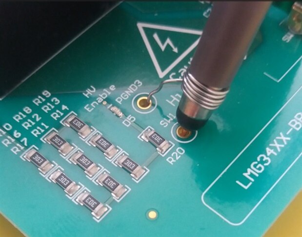
The series will use high-voltage FETs in half-bridge configuration.

This time I look at the bridge's output signal.

image

I'm particularly interested in the overshoot, because controlling that is one of the claimed advantages of GaN technology.


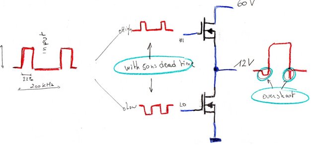
The high and low side of the bridge are controlled by an opposite signal. Both signals have a dead time inserted when one signal goes low and the other switches high.

GaN semiconductors don't need a lot of dead time. The setup here is configured for a 50 ns band.


image

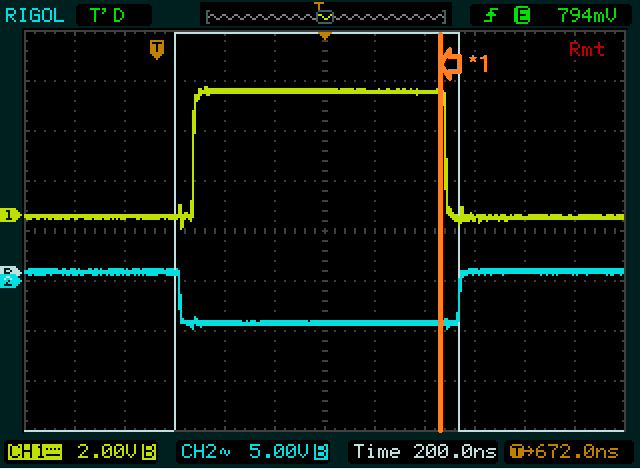
*1: I was sloppy when capturing this scope window. The falling edge of the input signal should be where the orange line is. Check comments below for more info.

Thank you jc2048 for spotting this.


The scope capture above shows the input (low-power) signals.

The white line is the input signal, with 22% duty cycle and a frequency of 200 kHz.

The yellow line is the driver signal for the high side FET, the blue signal for the low side one. Check the schematic below to get an idea of where the 3 signals occur.

(excuses for the mismatch in scope horizontal scale setting between yellow and blue. I only saw this after I disconnected my setup. They have the same amplitude.)


image


I'm going to probe the switcher's output signal. I'll zoom in on the overshoot positions, so you can see that the signal is behaving decently in the dead time.


image

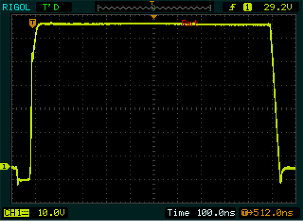
This trace is a full high part of the output at 200 kHz, 22% duty cycle.

It gives an impression of the switching artifacts just before the edges.


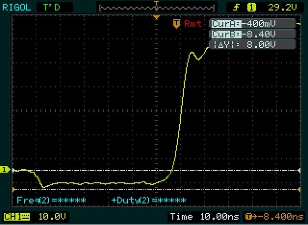
A detailed capture of the rising edge overshoot looks like this:

image

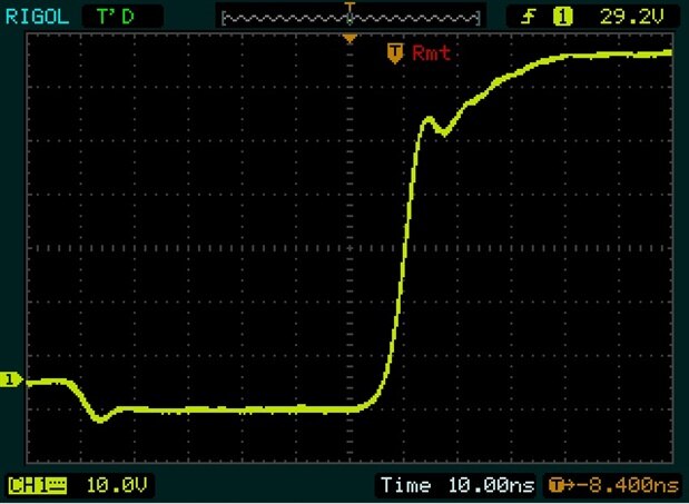
The input signal is 60 V. The overshoot is approximately -8 V:

image


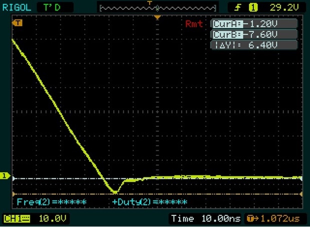
On the falling edge, there's less switching residue:

image

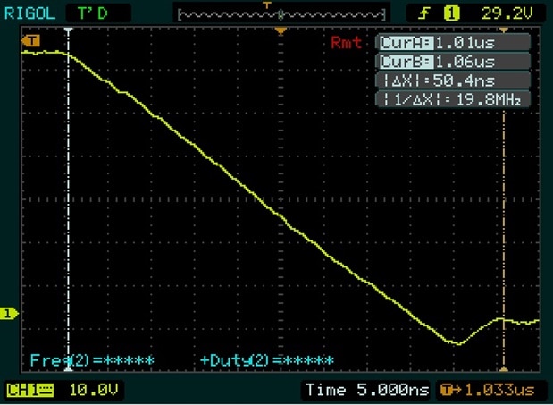
(the time scale is extended to the limits of what I can show on my scope screen. Check the full signal above to get an idea of how steep (50 ns) this ramp-down and overshoot is.)


image


The evaluation board that I'm using has reasonable filtering at the output. Let's check how the DC signal after that flter looks like.

image

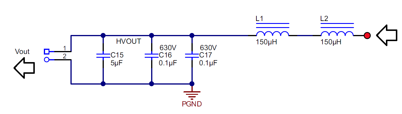
The load I'm using is approx. 12 W (12 V, 1 A). The capture below shows only the AC (noise) component of the output.

I get close to 650 mV of ripple peak-to-peak.

image


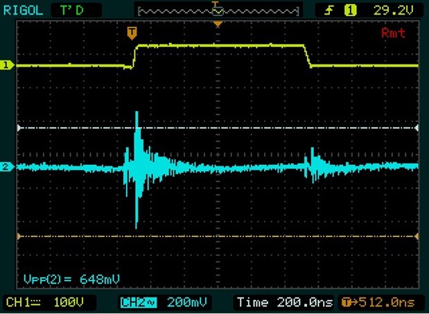
Not surprisingly, the largest artifacts appear at the edges of the PWM driver signals. This is a reasonable DC signal.

Further filtering will smoothen it more - the board I'm using is to show how the GaN FETs perform, so it doesn't focus on output filtering.


image


Part 1: Several 100 Volts
Part 2: Test Setup with LMG3410 Half-Bridge
Part 3: Probing the LMG3410 Half-Bridge
  • Sign in to reply

Top Comments

  • DAB
    DAB over 9 years ago +1
    Great update. I did have one thought, I wonder if the overshoot measurement was limited by your scopes bandwidth. Granted 50 nano seconds is not much, but I have seen femtosecond pulses destroy circuits…
  • jc2048
    jc2048 over 9 years ago +1
    Good stuff, Jan. Thanks for posting this. The high side FET anticipates the input signal and turns off 50nS before it arrives? Something tells me that might not be right. Line drawn in wrong place? I take…
  • Jan Cumps
    Jan Cumps over 9 years ago in reply to jc2048 +1
    I expect that if I would re-take the capture, and not exaggerate the saved input signal, the white signal would look like the (drawn by me in Paint ) red signal here:
  • Jan Cumps
    Jan Cumps over 7 years ago in reply to Jan Cumps

    Full desk:

    image


    This is a check with the input voltage at 30 V.

    Output 25.7 V

    Frequency 195 kHz

    228 mA current drawn.


    image


    The top 2 traces are the low and high signals for the half bridge, with deadband.

    Trace 3 is the switching node of the GAN FETs.

    Trace 4 is the output.

    • Cancel
    • Vote Up +1 Vote Down
    • Sign in to reply
    • More
    • Cancel
  • Jan Cumps
    Jan Cumps over 7 years ago in reply to Jan Cumps

    Rising edge, same scenario::


    1 A:


    image


    100 mA:


    image

    • Cancel
    • Vote Up +1 Vote Down
    • Sign in to reply
    • More
    • Cancel
  • Jan Cumps
    Jan Cumps over 7 years ago in reply to jc2048

    jc2048  wrote:


    I've just looked at the spec for your scope. It's very good value for money - I couldn't quite believe the price. But 50 MHz bandwidth is on the wrong side of marginal for this. [If anyone from element14 is reading this, we need a roadtest for a 1GHz scope with an active probe, please.]


    Traditionally, that would equate to a risetime spec of 0.35/fT = 0.35/50M = 7nS. Whether that applies to a sampled digital scope I don't know. It may do. The 1GSps is shared with the 100MHz version and gives enough oversampling that the traces should match an analogue scope fairly well if the sample timing is accurate and the signal processing is done nicely.


    It's not hopeless, but we need to be very skeptical about what you're seeing with the faster edges - that top GaN is turning on much faster than we think it is. And the shape of the waveform as it goes up is probably as much do with how a passive probe that matches a 50MHz scope behaves when it is hit by a 60V step with a rise time of a nanosecond or two (or maybe less) as what is going on in the circuit.


    The depiction of the falling edge is closer to the reality of what's happening in the circuit, so looking at different loads would still be interesting if you wanted to and had the time.


    I have done the exercise with a 100 MHz scope and different loads:.


    Load is 1 A:

    image


    Load is 100 mA:


    image


    I've used proper probing techniques this time, with the pigtail spring on the probe.

    • Cancel
    • Vote Up +1 Vote Down
    • Sign in to reply
    • More
    • Cancel
  • Jan Cumps
    Jan Cumps over 9 years ago in reply to jc2048

    Jon Clift wrote:


    I've just looked at the spec for your scope. It's very good value for money - I couldn't quite believe the price....

    I've purchased it second hand, it costed me the money I got for selling my old CRT scope + I believe 10€.

    • Cancel
    • Vote Up 0 Vote Down
    • Sign in to reply
    • More
    • Cancel
  • jc2048
    jc2048 over 9 years ago in reply to Jan Cumps

    I've just looked at the spec for your scope. It's very good value for money - I couldn't quite believe the price. But 50 MHz bandwidth is on the wrong side of marginal for this. [If anyone from element14 is reading this, we need a roadtest for a 1GHz scope with an active probe, please.]


    Traditionally, that would equate to a risetime spec of 0.35/fT = 0.35/50M = 7nS. Whether that applies to a sampled digital scope I don't know. It may do. The 1GSps is shared with the 100MHz version and gives enough oversampling that the traces should match an analogue scope fairly well if the sample timing is accurate and the signal processing is done nicely.


    It's not hopeless, but we need to be very skeptical about what you're seeing with the faster edges - that top GaN is turning on much faster than we think it is. And the shape of the waveform as it goes up is probably as much do with how a passive probe that matches a 50MHz scope behaves when it is hit by a 60V step with a rise time of a nanosecond or two (or maybe less) as what is going on in the circuit.


    The depiction of the falling edge is closer to the reality of what's happening in the circuit, so looking at different loads would still be interesting if you wanted to and had the time.

    • Cancel
    • Vote Up +1 Vote Down
    • Sign in to reply
    • More
    • Cancel
>
element14 Community

element14 is the first online community specifically for engineers. Connect with your peers and get expert answers to your questions.

  • Members
  • Learn
  • Technologies
  • Challenges & Projects
  • Products
  • Store
  • About Us
  • Feedback & Support
  • FAQs
  • Terms of Use
  • Privacy Policy
  • Legal and Copyright Notices
  • Sitemap
  • Cookies

An Avnet Company © 2026 Premier Farnell Limited. All Rights Reserved.

Premier Farnell Ltd, registered in England and Wales (no 00876412), registered office: Farnell House, Forge Lane, Leeds LS12 2NE.

ICP 备案号 10220084.

Follow element14

  • X
  • Facebook
  • linkedin
  • YouTube