


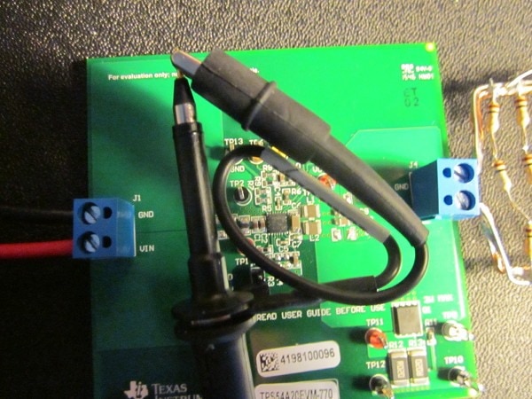
This is part five of evaluating a TPS54A20 on an evaluation board. The TPS54A20 is a buck converter with
an interesting topology - it has two phases merged with a switched-capacitor. This isn't a formal road
test (I was given the board by Jan Cumps, nice person that he is) and I'm just doing what interests me and
blogging about it. Disclaimer: some of what I do here is quite sloppy and, to be fair to TI, it shouldn't
be taken as a proper review.
This time I'm looking at the operation of the converter and specifically the role of the capacitor. See
this link for the discussion I had with Jan about the operation of the part - I won't repeat the details
here.
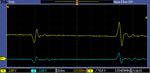
Here are the waveforms at each end of the capacitor with a load of about 9.5A. The low side (blue trace)
switches between 0 and 6 volts and the high side (yellow trace) between 6 and 12V. The input voltage is
12V. These traces were taken with the probes using the flying-lead ground and the pieces of wire that Jan
had soldered onto the ends of the capacitor.

The voltage across the capacitor is the difference between the two and you can see that on average it's
around 6 volts. After the trigger point, where both waveforms are high, you can see that the capacitor is
charging - the traces are diverging so the capacitor voltage is increasing. There is then a section where
the traces remain horizontal, followed by a third section where the traces close up - the capacitor is
discharging here and powering the other phase of the converter.
Here is the high part in more detail. (An obvious question is where does all the ringing come from?)

And here is the discharge section in more detail.
Here's the high part again but with spring clips for the ground rather than the flying lead (but Jan's
wires are still attached). The ringing is still there, but it's much more regular now. There are about 7
cycles in 40nS, so that's a frequency of about 175MHz. What I'm now struggling with is, how much is that
down to my probes and how much down to the circuit?

At this point I got diverted a bit and took a capture with the persistance set to infinity (though, needless to say, I didn't
wait for an infinite amount of time before stopping it - this is about 5 seconds worth, which will be a
few thousand captures). This shows us the jitter on the width which looks quite bad until you look at the
timebase and realise that it's not much more than 10nS.

This final trace is with Jan's wires removed, so is the best I can do with my passive probes.

The spring-clip grounds don't eliminate the lead inductance, they just reduce it compared to the flying
leads and push up the frequency at which we'll see ringing if the probe is hit by a fast edge [the
frequency is largely defined by the inductance and the various capacitances at the probe tip which form a
tuned circuit]. But what I can see here is far in excess of what I'd see probing fast logic, so it has to be
real. Unfortunately, it's also a prime EMC hazard - 175MHz is just nice for finding its way around
and radiating off of wiring and given the kinds of currents involved there's plenty of power.
Here's what I pick up with an informal and rather crude near-field probe (it consists of loop made from
the flying earth lead shorted to the probe tip)

It doesn't tell us anything about the levels (no calibration and you can't simply extrapolate from a
near-field measurement of the magnetic field to what happens further out anyway) but it does show that
there is something there. Shame I haven't saved up enough money for a spectrum analyser yet.
Top Comments