element14 Community
element14 Community
    Register Log In
  • Site
  • Search
  • Log In Register
  • Members
    Members
    • Achievement Levels
    • Benefits of Membership
    • Feedback and Support
    • Members Area
    • Personal Blogs
    • What's New on element14
  • Learn
    Learn
    • eBooks
    • Learning Center
    • Learning Groups
    • STEM Academy
    • Webinars, Training and Events
  • Technologies
    Technologies
    • 3D Printing
    • Experts & Guidance
    • FPGA
    • Industrial Automation
    • Internet of Things
    • Power & Energy
    • Sensors
    • Technology Groups
  • Challenges & Projects
    Challenges & Projects
    • Arduino Projects
    • Design Challenges
    • element14 presents
    • Project14
    • Project Groups
    • Raspberry Pi Projects
  • Products
    Products
    • Arduino
    • Avnet Boards Community
    • Dev Tools
    • Manufacturers
    • Product Groups
    • Raspberry Pi
    • RoadTests & Reviews
  • Store
    Store
    • Visit Your Store
    • 'Choose another store...'
      • Europe
      •  Austria (German)
      •  Belgium (Dutch, French)
      •  Bulgaria (Bulgarian)
      •  Czech Republic (Czech)
      •  Denmark (Danish)
      •  Estonia (Estonian)
      •  Finland (Finnish)
      •  France (French)
      •  Germany (German)
      •  Hungary (Hungarian)
      •  Ireland
      •  Israel
      •  Italy (Italian)
      •  Latvia (Latvian)
      •  
      •  Lithuania (Lithuanian)
      •  Netherlands (Dutch)
      •  Norway (Norwegian)
      •  Poland (Polish)
      •  Portugal (Portuguese)
      •  Romania (Romanian)
      •  Russia (Russian)
      •  Slovakia (Slovak)
      •  Slovenia (Slovenian)
      •  Spain (Spanish)
      •  Sweden (Swedish)
      •  Switzerland(German, French)
      •  Turkey (Turkish)
      •  United Kingdom
      • Asia Pacific
      •  Australia
      •  China
      •  Hong Kong
      •  India
      •  Korea (Korean)
      •  Malaysia
      •  New Zealand
      •  Philippines
      •  Singapore
      •  Taiwan
      •  Thailand (Thai)
      • Americas
      •  Brazil (Portuguese)
      •  Canada
      •  Mexico (Spanish)
      •  United States
      Can't find the country/region you're looking for? Visit our export site or find a local distributor.
  • Translate
  • Profile
Personal Blogs
  • Members
  • More
Personal Blogs
Legacy Personal Blogs Transistors: Vbe Reverse Breakdown
  • Blog
  • Documents
  • Mentions
  • Sub-Groups
  • Tags
  • More
  • Cancel
  • New
Blog Post Actions
  • Subscribe by email
  • More
  • Cancel
  • Share
  • Subscribe by email
  • More
  • Cancel
Group Actions
  • Group RSS
  • More
  • Cancel
Engagement
  • Author Author: jc2048
  • Date Created: 12 Feb 2017 7:10 PM Date Created
  • Views 3194 views
  • Likes 6 likes
  • Comments 20 comments
Related
Recommended

Transistors: Vbe Reverse Breakdown

jc2048
jc2048
12 Feb 2017

A further blog in my series about transistors [I think I've given myself a lifetime job, mining this rich seam]. This

one looks at the reverse breakdown of the base-emitter junction and one application of the transistor if it's used in

this way [actually, I only know of one application, but no doubt D_Hersey will be along in a while to quote half a

dozen from the Electropedia that sits inside his head].


On a datasheet the maximum figure for this junction is often given as 5V or 6V (for the kind of silicon, small-signal,

bipolar junction transistor that I'm using in my experiments).


image

Obviously, the manufacturer gives themselves some leeway, so the actual breakdown voltage is going to be several volts

greater than that. Unlike the case of the collector-emitter breakdown blog, where I used a switching circuit with an

inductor, here I'm just going to treat the junction as though it were a zener diode and put a resistor in series to

limit the current. These test circuits are getting simpler and simpler.


Here's the circuit:

image

The simulation just reported that the voltage at the transistor-resistor node was 12V, so it doesn't model the

breakdown (at least, not for the 2N3904 part that I selected from the library).


Before I try it, I'm going to do something that won't necessarily make much sense now, but you'll understand why I've

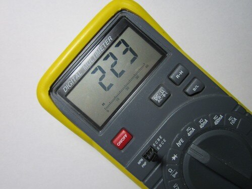
done it a bit further down; I'm going to measure the beta of the part [I haven't done beta yet - talk about

unstructured blogging - but it's the DC current gain of the transistor, the ratio of collector current to base current

measured at a particular collector current, and on a datasheet it's often referred to as hFE - I haven't done hybrid

models either yet, but if I keep throwing in these little morsels it'll all seem quite natural and familiar when I

eventually do]. Here is what my cheap meter with a transistor test facility says for the gain:


image


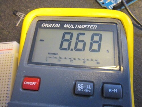
Here are the results of the reverse breakdown:


image


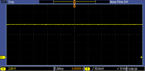
and here's what it looks like on an oscilloscope:


image


So I've got myself an 8.7V zener.


Now I've had the transistor running like that for 10 minutes, I'm going to take it out of circuit and measure the beta

again. What we can see is that the breakdown has done some damage to the device and affected the gain.


image


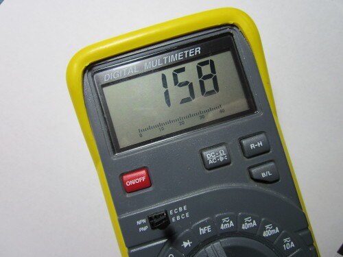
I have read in books that there's a certain amount of recovery of the gain afterwards, but I'm not seeing that with

this device; several hours later it is still reading 158.


Noise


We haven't had any Shakespeare for a while, so a quick quotation


"Be not afeard; the isle is full of noises, ..."
William Shakespeare. Tempest [III, 2]


The one application that I know of for the reverse base-emitter breakdown is as a noise diode. The avalanche effect is

quite noisy and chaotic, and if it's ac coupled and amplified it makes a reasonable white noise source, so I'm going

to try that here. Apparently, transistors vary widely in the amplitude of the noise they generate in this way, so if

you were doing this for real you'd probably buy a batch and pick out the 'good' ones. I just want to look at it and

see it there, so I'll keep working with the device I've been experimenting with - but bear in mind it might not be

very typical.


Here's the noise, as seen by my scope. Unfortunately, that's the best the scope can do.


image


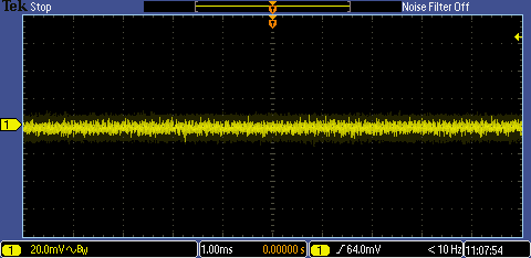
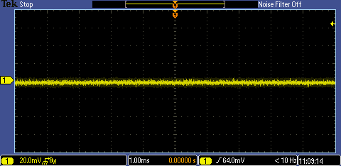
Before you go away with the idea that all of that comes from the emitter-base breakdown, here's what the scope shows

when the input is set to ground.


image


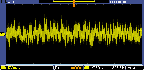
So that I could look at the noise in a bit more detail, I assembled a simple gain stage from a pair of TL081s on a

breadboard - I gave each a gain of 10, so overall this is one hundred times the noise generated by the transistor. I

also modified the simple circuit of the transistor and resistor by substituting a simple current source for the

resistor, since in the original form it wasn't too happy driving the amplifier.


Here's a single trace of the noise (if you're attentive, you'll see that mixed in with the noise is something that

looks a bit more regular and that's because the circuit is picking up some interference).


image


And here's the accumulated trace.


image


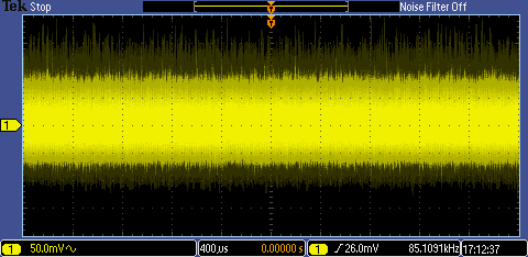
It looks a bit biassed one way (the view is ac coupled), so the noise isn't symmetrical, which probably reflects the

physical basis of its generation. I could probably have done this a bit better, but it gives an idea of how it coud be

used as a noise source with a bit of work.

  • Sign in to reply

Top Comments

  • jc2048
    jc2048 over 6 years ago in reply to jc2048 +4
    I had another go, but still can't give an answer. I couldn't swap the meters because I needed the good one to be where it was to be in with a chance of reading the low currents, so I put a follower (OP177…
  • mcb1
    mcb1 over 6 years ago +3
    Every time I hooked them up backwards, it was unintentional. Usually the magic smoke exited left, so the gain was seriously changed. Mark
  • jc2048
    jc2048 over 6 years ago in reply to mcb1 +3
    I now have a theory that the symbol that you, Jan Cumps and rachaelp have after your names is a smoke detector going off...
Parents
  • dougw
    dougw over 6 years ago

    This transistor series has lots of interest. Thanks.

    I have heard that the knee of the B-E reverse breakdown (although noisy) is sharper than a normal zener. But I have not tested this assertion.

    Do you also get a similar reverse (but higher voltage) breakdown of the B-C junction?

    • Cancel
    • Vote Up +1 Vote Down
    • Sign in to reply
    • More
    • Cancel
  • jc2048
    jc2048 over 6 years ago in reply to dougw

    Interesting questions that I don't (yet) know the answer to. It may take a day or two - I'm a bit busy with things at the moment.

    • Cancel
    • Vote Up +1 Vote Down
    • Sign in to reply
    • More
    • Cancel
  • jc2048
    jc2048 over 6 years ago in reply to jc2048

    I had a go at measuring the characteristic, took lots of readings, felt pleased with myself and did the graph, came up with the following curve (in blue), wondered why it looked the shape it did, and then realised that at the low end I was measuring the characteristic of the volt meter (10M input). If I have time later, I'll swap the meters, put the good one on the voltage, and do it all again. What an old fool I am!


    I think the B-C breakdown is the Vce one less a diode drop.


    image

    • Cancel
    • Vote Up +2 Vote Down
    • Sign in to reply
    • More
    • Cancel
Comment
  • jc2048
    jc2048 over 6 years ago in reply to jc2048

    I had a go at measuring the characteristic, took lots of readings, felt pleased with myself and did the graph, came up with the following curve (in blue), wondered why it looked the shape it did, and then realised that at the low end I was measuring the characteristic of the volt meter (10M input). If I have time later, I'll swap the meters, put the good one on the voltage, and do it all again. What an old fool I am!


    I think the B-C breakdown is the Vce one less a diode drop.


    image

    • Cancel
    • Vote Up +2 Vote Down
    • Sign in to reply
    • More
    • Cancel
Children
No Data
element14 Community

element14 is the first online community specifically for engineers. Connect with your peers and get expert answers to your questions.

  • Members
  • Learn
  • Technologies
  • Challenges & Projects
  • Products
  • Store
  • About Us
  • Feedback & Support
  • FAQs
  • Terms of Use
  • Privacy Policy
  • Legal and Copyright Notices
  • Sitemap
  • Cookies

An Avnet Company © 2023 Premier Farnell Limited. All Rights Reserved.

Premier Farnell Ltd, registered in England and Wales (no 00876412), registered office: Farnell House, Forge Lane, Leeds LS12 2NE.

ICP 备案号 10220084.

Follow element14

  • X
  • Facebook
  • linkedin
  • YouTube