element14 Community
element14 Community
    Register Log In
  • Site
  • Search
  • Log In Register
  • Members
    Members
    • Benefits of Membership
    • Achievement Levels
    • Members Area
    • Personal Blogs
    • Feedback and Support
    • What's New on element14
  • Learn
    Learn
    • Learning Center
    • eBooks
    • STEM Academy
    • Webinars, Training and Events
    • More
  • Technologies
    Technologies
    • 3D Printing
    • FPGA
    • Industrial Automation
    • Internet of Things
    • Power & Energy
    • Sensors
    • More
  • Challenges & Projects
    Challenges & Projects
    • Design Challenges
    • element14 presents
    • Project14
    • Arduino Projects
    • Raspberry Pi Projects
    • More
  • Products
    Products
    • Arduino
    • Dev Tools
    • Manufacturers
    • Raspberry Pi
    • RoadTests & Reviews
    • Avnet Boards Community
    • More
  • Store
    Store
    • Visit Your Store
    • Choose Another Store
      • Europe
      •  Austria (German)
      •  Belgium (Dutch, French)
      •  Bulgaria (Bulgarian)
      •  Czech Republic (Czech)
      •  Denmark (Danish)
      •  Estonia (Estonian)
      •  Finland (Finnish)
      •  France (French)
      •  Germany (German)
      •  Hungary (Hungarian)
      •  Ireland
      •  Israel
      •  Italy (Italian)
      •  Latvia (Latvian)
      •  
      •  Lithuania (Lithuanian)
      •  Netherlands (Dutch)
      •  Norway (Norwegian)
      •  Poland (Polish)
      •  Portugal (Portuguese)
      •  Romania (Romanian)
      •  Russia (Russian)
      •  Slovakia (Slovak)
      •  Slovenia (Slovenian)
      •  Spain (Spanish)
      •  Sweden (Swedish)
      •  Switzerland(German, French)
      •  Turkey (Turkish)
      •  United Kingdom
      • Asia Pacific
      •  Australia
      •  China
      •  Hong Kong
      •  India
      •  Korea (Korean)
      •  Malaysia
      •  New Zealand
      •  Philippines
      •  Singapore
      •  Taiwan
      •  Thailand (Thai)
      • Americas
      •  Brazil (Portuguese)
      •  Canada
      •  Mexico (Spanish)
      •  United States
      Can't find the country/region you're looking for? Visit our export site or find a local distributor.
  • Translate
  • Profile
Personal Blogs
  • Members
  • More
Personal Blogs
Douglas Wong's Blog Strip Board - Is it the best prototyping board?
  • Blogs
  • Documents
  • Mentions
  • Sub-Groups
  • Tags
  • More
  • Cancel
  • New
Blog Post Actions
  • Subscribe by email
  • More
  • Cancel
  • Share
  • Subscribe by email
  • More
  • Cancel
Group Actions
  • Group RSS
  • More
  • Cancel
Engagement
  • Author Author: dougw
  • Date Created: 23 Aug 2021 3:17 AM Date Created
  • Views 1253 views
  • Likes 20 likes
  • Comments 27 comments
  • veroboard
  • doug wong
  • track cutter
  • spotface cutter
  • strip board
  • proto board
Related
Recommended

Strip Board - Is it the best prototyping board?

dougw
dougw
23 Aug 2021

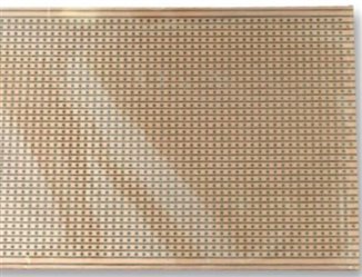
Veroboard

Spoiler alert - for me strip board is generally the best proto-board. But why?

Well, when it comes to circuit cards, I have a compulsion to make them clean, neat and orderly (PCB-OCD).

I have all these rules and objectives that I use when laying out circuit cards that have little to do with circuit functionality and everything to do with my concept of an aesthetically pleasing layout.

I have no idea what courses teach with regards to layout aesthetics since I never took such a course, but some of my rules come from the days before CAD when I was laying out PCBs using translucent red and blue tape.

For example I try hard to minimize the number of vias because every drilled hole increases costs.

I also try to ensure the maximum number of straight line connections since making a corner with tape takes at least twice as much time.

Re-spinning cards was (and is) a big no-no since it doubles costs and causes big delays. If you have ever had to rip up layers of tape to fix a layout issue, you know how painful it can get and why I have such an aversion to it.

In the past 400 or so PCBs I have designed, approximately 1 card needed to be re-spun (due to an idiotic assumption about pin assignments).

Approximate because I have re-spun some cards, but usually to add new features or because I wanted to improve the circuit. However I also design PCBs to allow circuit improvement without spinning a new card.

So what does this have to do with strip board?

The alternative proto boards to strip board all seem to end up with higglety-pigglety point-to-point wiring that for some reason offends my sense of propriety, even though they work perfectly well.

To digress for one point, the big promise of double sided PCBs is that all connections can be 100% routed without requiring any jumpers, even if different nets need to cross each other without touching. The simple paradigm is that all traces on one side of the card run in the same direction and all traces on the other side of the card run at 90 degrees. This allows traces to cross each other without touching simply by using vias to get to the other side of the card and hop over the track.

Strip board implements this paradigm by including all the traces on the bottom of the card running in the same direction and has all the vias pre-drilled to allow jumper connections across traces. In practice, through-hole components bridge between traces, so very few jumpers are actually needed. Basically all nets have a horizontal trace or section of a trace on the bottom of the card and all components are installed vertically between these nets. It can end up looking as neat and almost as dense as a custom double-sided PCB. It takes some planning to efficiently use the horizontal traces on the bottom and minimize vertical jumpers, but the result can be a very clean circuit card. For example the power and ground nets are generally horizontal traces that run the length of the card. Many components directly connect to these  bus bars. Also if there are busses involved they are already built into the strip board.

Individual nets may only have a few components connected, so they only need to occupy a short trace on the copper side. The trace is cut using a spot-face cutter so that the next section of the same trace can be used for another net.

Example Circuit

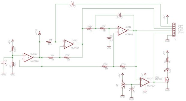
Here is a simple schematic of a quad op-amp chip with 19 other components implementing standard topologies for an amplifier, a filter and a comparator.

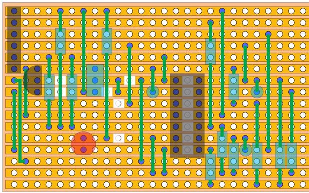
Here is top-view with transparency of what it might look like wired on a stripboard. The white squares are where the tracks get cut on the copper side. You can see it keeps point-to-point wiring clutter to a minimum.

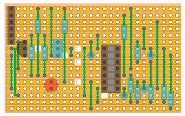
After Jon Clift pointed out that there were connection errors, I made a new version with a bunch of changes....Incidentally, these changes could have been made on a real card without any change to the final look.

Here is the old one for those who are curious:


Newark carries lots of different sizes of stripboard or VeroBoard and they even carry a tool to cut the trackstool to cut the tracks.

As you use stripboard more, you discover lots of ways to make your prototyping easier and better looking. For example it lends itself well to be used with wire-wrap sockets and 0.1" pitch headers.

There are lots of breakout cards for SMT devices that use 0.1" pitch headers that work well with stripboard.

It would even directly connect to my BBC-PCBs which provide a variety of interface connectors.

I have developed several techniques to plan stripboard layouts using either graph paper, a spreadsheet or my regular CAD software. They are not really complete enough to be full solutions since I use them in conjunction with all my knowledge, but they help me to avoid getting jammed with not enough space.

I toyed with the idea of making a stripboard CAD program that would simplify the process, but I no longer do enough stripboard to make that exercise worthwhile.

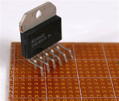
Stripboards can even connect some difficult to connect parts like this big H-bridge that do not use 0.1" pitch for their pins - this one just needs to be placed at 45 degrees and each pin ends up on a different track, assuming you cut the appropriate tracks between pins.

Summary

I don't use a lot of prototyping cards now, but I have in the past and when I need to use prototyping cards, my go to style is stripboard. Hands down I find it to be easier to work with and the resulting circuit board looks better.

I haven't ever seen a course on how to effectively use stripboard, but it is something that can benefit makers if they take time to learn how to incorporate it into their workflows.

There are a few YouTube videos on stripboard, but from what I've seen they don't cover all the benefits (this blog doesn't either).

If you have a preferred style of prototyping card, explain it in the comments below.

Anonymous

Top Comments

  • jc2048
    jc2048 8 months ago +9

    I can spot two errors in your stripboard layout, if anyone wants to try practising their fault-finding skills.


    You were lucky with the transparent red and blue tape: the first company I worked for was really…

  • shabaz
    shabaz 8 months ago +9

    Also I guess people are familiar with the Eloi/Morlock capability with these boards : ) Like the lower stripboard only seems to have about 6 parts..

    But on the underside there's at least another 16 components…

  • 14rhb
    14rhb 8 months ago +7

    A great blog reminding me of when I got started in electronics mid 80's. Unfortunately some interesting modern devices don't come with 0.1" friendly pin outs, although a small SMT/SOIC etc breakout can…

Parents
  • jc2048
    jc2048 8 months ago

    I can spot two errors in your stripboard layout, if anyone wants to try practising their fault-finding skills.


    You were lucky with the transparent red and blue tape: the first company I worked for was really cheap and we only had black crepe tape to work with. Did you get to use transfers like these for the DIL chips, or did you use the circular component-lead pads?


    • Cancel
    • Up +9 Down
    • Reply
    • More
    • Cancel
  • dougw
    dougw 8 months ago in reply to jc2048

    Yes we had a number of different pad decals in black as well as black tape for when both sides had copper. I still have a box of tape somewhere - will have to dig it out.

    Yes the layout is not tested and is not optimized - it is just to provide some insight into what the final layout might look like. One missed track cut stands out.

    • Cancel
    • Up +6 Down
    • Reply
    • More
    • Cancel
  • jc2048
    jc2048 8 months ago in reply to dougw

    I think there's a second missed track cut.


    To answer the your original question, I will sometimes prototype on stripboard, but I like much more building ad-hoc on raw pcb material cut into islands with a craft knife.


    The stripboard example, on the right, was an ADC with a simple, passive reconstruction filter. I chose the stripboard because there are headers underneath that plug into a Brevia 2 FPGA board and it would have been very messy to try and do that without the neat 0.1" grid of holes. The pcb board example, on the left, was for one of my 'experimenting' blogs, can't remember which one, and the circuit grew and developed (in 3 dimensions - there's an upside-down chip in the bottom-left corner) as I went along.

    • Cancel
    • Up +5 Down
    • Reply
    • More
    • Cancel
  • dougw
    dougw 8 months ago in reply to jc2048

    Cool - busses on the base and nets in space...

    • Cancel
    • Up +3 Down
    • Reply
    • More
    • Cancel
  • Jan Cumps
    Jan Cumps 8 months ago in reply to jc2048

    jc2048  wrote:


    ... I chose the stripboard because there are headers underneath...

    I have the same preference. Cladboard as first choice. stripboard (with or without lanes) when using headers.

    I prefer the simple stripboards (long lanes, all pads in a lane connected) more than the ones with elaborated trace schemes.

    • Cancel
    • Up +5 Down
    • Reply
    • More
    • Cancel
Comment
  • Jan Cumps
    Jan Cumps 8 months ago in reply to jc2048

    jc2048  wrote:


    ... I chose the stripboard because there are headers underneath...

    I have the same preference. Cladboard as first choice. stripboard (with or without lanes) when using headers.

    I prefer the simple stripboards (long lanes, all pads in a lane connected) more than the ones with elaborated trace schemes.

    • Cancel
    • Up +5 Down
    • Reply
    • More
    • Cancel
Children
No Data
Element14

element14 is the first online community specifically for engineers. Connect with your peers and get expert answers to your questions.

  • Members
  • Learn
  • Technologies
  • Challenges & Projects
  • Products
  • Store
  • About Us
  • Feedback & Support
  • FAQs
  • Terms of Use
  • Privacy Policy
  • Legal and Copyright Notices
  • Sitemap
  • Cookies

An Avnet Company © 2022 Premier Farnell Limited. All Rights Reserved.

Premier Farnell Ltd, registered in England and Wales (no 00876412), registered office: Farnell House, Forge Lane, Leeds LS12 2NE.

ICP 备案号 10220084.

Follow element14

  • Facebook
  • Twitter
  • linkedin
  • YouTube