element14 Community
element14 Community
    Register Log In
  • Site
  • Search
  • Log In Register
  • Community Hub
    Community Hub
    • What's New on element14
    • Feedback and Support
    • Benefits of Membership
    • Personal Blogs
    • Members Area
    • Achievement Levels
  • Learn
    Learn
    • Ask an Expert
    • eBooks
    • element14 presents
    • Learning Center
    • Tech Spotlight
    • STEM Academy
    • Webinars, Training and Events
    • Learning Groups
  • Technologies
    Technologies
    • 3D Printing
    • FPGA
    • Industrial Automation
    • Internet of Things
    • Power & Energy
    • Sensors
    • Technology Groups
  • Challenges & Projects
    Challenges & Projects
    • Design Challenges
    • element14 presents Projects
    • Project14
    • Arduino Projects
    • Raspberry Pi Projects
    • Project Groups
  • Products
    Products
    • Arduino
    • Avnet Boards Community
    • Dev Tools
    • Manufacturers
    • Multicomp Pro
    • Product Groups
    • Raspberry Pi
    • RoadTests & Reviews
  • Store
    Store
    • Visit Your Store
    • Choose another store...
      • Europe
      •  Austria (German)
      •  Belgium (Dutch, French)
      •  Bulgaria (Bulgarian)
      •  Czech Republic (Czech)
      •  Denmark (Danish)
      •  Estonia (Estonian)
      •  Finland (Finnish)
      •  France (French)
      •  Germany (German)
      •  Hungary (Hungarian)
      •  Ireland
      •  Israel
      •  Italy (Italian)
      •  Latvia (Latvian)
      •  
      •  Lithuania (Lithuanian)
      •  Netherlands (Dutch)
      •  Norway (Norwegian)
      •  Poland (Polish)
      •  Portugal (Portuguese)
      •  Romania (Romanian)
      •  Russia (Russian)
      •  Slovakia (Slovak)
      •  Slovenia (Slovenian)
      •  Spain (Spanish)
      •  Sweden (Swedish)
      •  Switzerland(German, French)
      •  Turkey (Turkish)
      •  United Kingdom
      • Asia Pacific
      •  Australia
      •  China
      •  Hong Kong
      •  India
      •  Korea (Korean)
      •  Malaysia
      •  New Zealand
      •  Philippines
      •  Singapore
      •  Taiwan
      •  Thailand (Thai)
      • Americas
      •  Brazil (Portuguese)
      •  Canada
      •  Mexico (Spanish)
      •  United States
      Can't find the country/region you're looking for? Visit our export site or find a local distributor.
  • Translate
  • Profile
  • Settings
Personal Blogs
  • Community Hub
  • More
Personal Blogs
Frank Milburn's Blog JFET Static Charge Detector
  • Blog
  • Documents
  • Mentions
  • Sub-Groups
  • Tags
  • More
  • Cancel
  • New
  • Share
  • More
  • Cancel
Group Actions
  • Group RSS
  • More
  • Cancel
Engagement
  • Author Author: fmilburn
  • Date Created: 22 Aug 2021 4:02 AM Date Created
  • Views 5630 views
  • Likes 13 likes
  • Comments 9 comments
  • detector
  • electrostatic_discharge
  • jfet
  • static
  • led
  • esd
Related
Recommended

JFET Static Charge Detector

fmilburn
fmilburn
22 Aug 2021

In a recent element14 Essentials on Static Control, shabaz said this:  "A 2N3819 + meter or LED makes a nice simple charge detector too : )"


So, I thought I would try it.  I don't have a 2N3819 but I do have a J112 N-channel JFET.  The circuit is shown below:

image

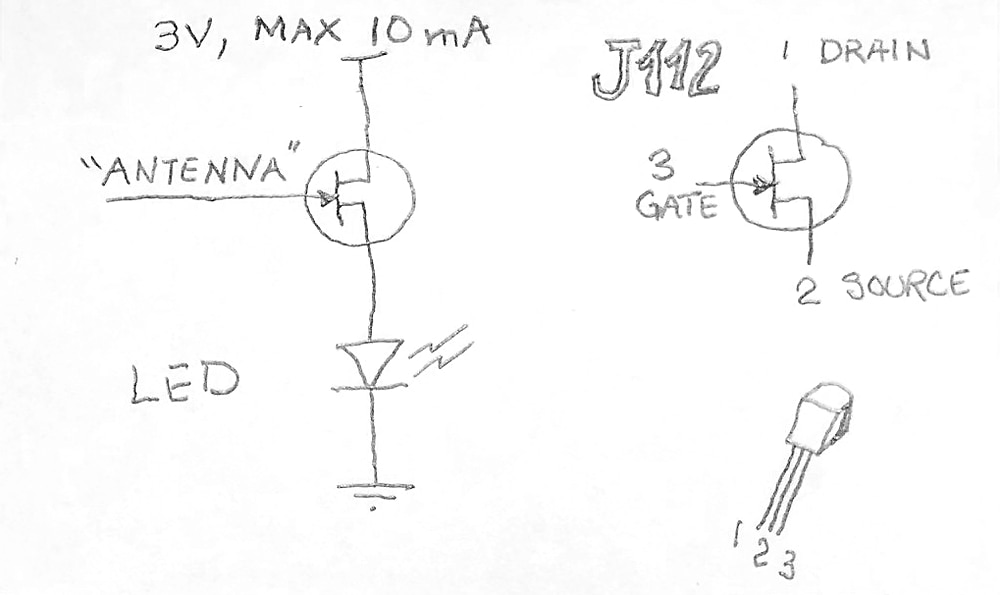
Power is supplied by a bench power supply set to 3V current limited to 10mA.  The "antenna" is a 5-inch long piece of wire.


So how does it work?  A JFET has extremely high input impedance - hardly any current flows into the gate - it is voltage controlled.  Current flow from drain to source is determined by the voltage differential between the gate and the source.  The drain to source current flow is highest when the gate to source voltage differential is zero.  As the gate to source voltage differential becomes more negative the drain to source current flow decreases.  At the pinch-off (sometimes called cutoff) voltage the drain to source current essentially ceases.  In the detector circuit, the gate/antenna becomes negative relative to the source and the FET turns the LED off gradually as the statically charged object comes closer.  I demonstrate it in the following 40-second video:


You don't have permission to edit metadata of this video.
Edit media
x
image
Upload Preview
image


As one of the resident mechanical engineers who has never seen this demonstrated, I was suitably impressed.  Comments and corrections to my understanding are always welcome image

  • Sign in to reply

Top Comments

  • shabaz
    shabaz over 3 years ago +4
    Hi Frank, Awesome results! It's definitely a fun experiment too. Great diagram too by the way!!
  • jc2048
    jc2048 over 3 years ago +3
    Good experiment and demonstration. The drain to source current flow is highest when the gate to source voltage differential is zero. Although this is obviously nit-picking, I think you'd find, if you tried…
  • fmilburn
    fmilburn over 3 years ago in reply to jc2048 +3
    Good points and thanks for the comments... I originally used the word "positive" instead of zero. But one of my references stated the gate should not be biased positive so I changed it to zero. Your explanation…
Parents
  • jc2048
    jc2048 over 3 years ago

    Good experiment and demonstration.


    The drain to source current flow is highest when the gate to source voltage differential is zero.

    Although this is obviously nit-picking, I think you'd find, if you tried it, that it would keep increasing as you went above zero. Obviously, at some point, the gate-source diode is going to start to become forward-biased and spoil things by conducting, but you'd probably have a small amount of leeway before that happened.


    In the detector circuit, the gate/antenna becomes negative relative to the source...

    That's a bit vague. How does it become negative? Are you claiming that the statically-charged object adds negative charge to the gate/antenna? An alternative hypothesis might be that it causes a redistribution of the free electrons in the wire, so that there's a greater concentration down the gate end.

    • Cancel
    • Vote Up +3 Vote Down
    • Sign in to reply
    • More
    • Cancel
  • fmilburn
    fmilburn over 3 years ago in reply to jc2048

    Good points and thanks for the comments...  I originally used the word "positive" instead of zero.  But one of my references stated the gate should not be biased positive so I changed it to zero.  Your explanation makes the reasoning for doing that and the true behavior clear.


    I researched how the gate/antenna works on the internet before writing but most of what I found made no sense and seemed like hand-waving blather.  I couldn't find anything in my textbooks.  Not wanting to add to the misinformation on the internet I made it vague.  In truth, I don't know the physics but it seems more likely that electrons are redistributed in the wire than that they are somehow transferred to the wire.  I like your explanation.

    • Cancel
    • Vote Up +3 Vote Down
    • Sign in to reply
    • More
    • Cancel
  • jc2048
    jc2048 over 3 years ago in reply to fmilburn

    I couldn't find anything in my textbooks.

    I'm no academic, and my physics is a bit dodgy at times, but perhaps we might describe what you've got as an irregular capacitor. For the 'old' physics models, that us engineers use, you'd be looking at a text on electricity and magnetism, and specifically electrostatics, electric fields, and capacitance.


    The eraser is one 'plate', with an excess of trapped charge, the wire the other, with charge able to move beyond the capacitor but only within the confines of the length of wire, so all to do with 'end effects' and little regular capacitor theory. It's really more about how the electric field arranges itself in space and then changes as the free charge in the wire drifts as a reaction to it. Trying to calculate anything with regular capacitor models would be horrendous - textbook examples of capacitance always consider very simple structures with lots of symmetry - so here you'd probably use finite-element methods, in a similar way as is used for the fields around an antenna, and rely on the ability of a computer to do lots of calculations very quickly, but to do that you'd need a 3-d model of the structure to work with, and it would have to be run through multiple iterations [dividing time into discrete intervals] with all the usual worries about accumulated errors and so on, until it reached an equilibrium.


    In practice it's much simpler to just do what you did and try it. Or think about it in a hand-wavy way, like I did, and imagine roughly how the electrons in the wire are going to behave simply from an electrostatic point of view. I did it backwards. You told me that the potential at the gate dropped, so a surfeit of electrons, driven down by the charge on the eraser, which in turn must be an excess of electrons. Simples! - as the interwibblers say [or maybe used to say - I don't make any effort to keep up].


    Keep in mind that the JFET will be prone to some leakage across the reverse-biased junction, so if you leave the eraser close to the wire, the gate potential will slowly change as charge leaves the wire. (Increasing the reverse potential will encourage more leakage.) But the JFET has a neat 'reset' mechanism - think what happens if you let the gate get back close to zero and then remove the eraser again.


    But, having said all that, a further thing to keep solidly in mind with any experiment like this, done in an inside environment, is the prevalence of mains fields. Your hand will distort those fields and it's quite possible that the effect you're seeing derives from that rather than the charge on the eraser. You would need to experiment further to show that it was the eraser causing the effect.


    Finally, to continue the glorious tradition of polluting the interknots, the water analogy might be something like this: the eraser as the moon, the wire as a tidal river, and the JFET as a port where the boats sit on the mud at low tide. It doesn't quite work, but no worse than the 'capacitor as a bucket of water' kind of tosh.

    • Cancel
    • Vote Up +3 Vote Down
    • Sign in to reply
    • More
    • Cancel
  • shabaz
    shabaz over 3 years ago in reply to jc2048

    Hi Jon,


    Unrelated (well, slightly related although it's not fully 3D for the situation here) I found this cool free software yesterday, called atlc2 that allows to determine the capacitance of any arbitrary cross-sections of conductors, and in the presence of any arbitrary shape cross-section dielectrics. I think it can't do arbitrary 3D shape though, perhaps that requires a supercomputer.. but nevertheless even 2D is useful.

    Here's my first attempt with it. The input has to be a graphic file (.bmp) describing the cross-section. Here I drew the conductors as red and blue, simulating copper trace, on top of a slab of FR4. The colours have to be specific RGB values to represent particular materials.

    image


    Then, I told the program how many millimetres each pixel represented, and it thinks about it, and generates this diagram:


    image

    And it also spits out the capacitance, of (I'm pretty sure) 1m length of such a cross-section. Also the inductance of the red element of that length too. And characteristic impedance. From the limited time trying it, it's a really cool program : )

    image

    • Cancel
    • Vote Up +3 Vote Down
    • Sign in to reply
    • More
    • Cancel
Comment
  • shabaz
    shabaz over 3 years ago in reply to jc2048

    Hi Jon,


    Unrelated (well, slightly related although it's not fully 3D for the situation here) I found this cool free software yesterday, called atlc2 that allows to determine the capacitance of any arbitrary cross-sections of conductors, and in the presence of any arbitrary shape cross-section dielectrics. I think it can't do arbitrary 3D shape though, perhaps that requires a supercomputer.. but nevertheless even 2D is useful.

    Here's my first attempt with it. The input has to be a graphic file (.bmp) describing the cross-section. Here I drew the conductors as red and blue, simulating copper trace, on top of a slab of FR4. The colours have to be specific RGB values to represent particular materials.

    image


    Then, I told the program how many millimetres each pixel represented, and it thinks about it, and generates this diagram:


    image

    And it also spits out the capacitance, of (I'm pretty sure) 1m length of such a cross-section. Also the inductance of the red element of that length too. And characteristic impedance. From the limited time trying it, it's a really cool program : )

    image

    • Cancel
    • Vote Up +3 Vote Down
    • Sign in to reply
    • More
    • Cancel
Children
  • fmilburn
    fmilburn over 3 years ago in reply to shabaz

    That is an interesting UI - using color to specify material and pixel size for dimensions. Quick and easy image

    • Cancel
    • Vote Up +3 Vote Down
    • Sign in to reply
    • More
    • Cancel
element14 Community

element14 is the first online community specifically for engineers. Connect with your peers and get expert answers to your questions.

  • Members
  • Learn
  • Technologies
  • Challenges & Projects
  • Products
  • Store
  • About Us
  • Feedback & Support
  • FAQs
  • Terms of Use
  • Privacy Policy
  • Legal and Copyright Notices
  • Sitemap
  • Cookies

An Avnet Company © 2025 Premier Farnell Limited. All Rights Reserved.

Premier Farnell Ltd, registered in England and Wales (no 00876412), registered office: Farnell House, Forge Lane, Leeds LS12 2NE.

ICP 备案号 10220084.

Follow element14

  • X
  • Facebook
  • linkedin
  • YouTube