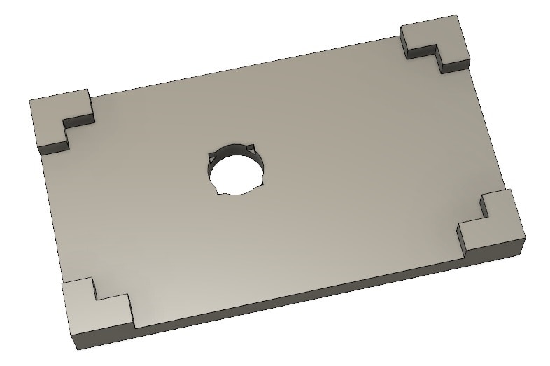
In my prior post (/members-area/personalblogs/b/gene-breniman-s-blog/posts/hand-soldering-a-vqfn24-part-to-a-pcb), I was very happy with the end result, but a little disappointed with the preciseness of the alignment of the chip on the board. So, as I had mentioned in that blog, I decided to redesign my soldering jig, using some of the available holes (pins and mounting) to align the board on to the fixture (as opposed to the board edges). In redesigning the fixture, I first removed the four corner retainers (first image) and shrunk down the overall size to match the PCB. I then extracted position information from my PCB design software (Eagle) for the location and sizes of the USB plug mounting holes and the three pin header on the opposite side of the PCB. With that information I fired up Fusion360 (after renewing my license) and added two prongs (USB plug) and three square holes (header) to the fixture (second image).
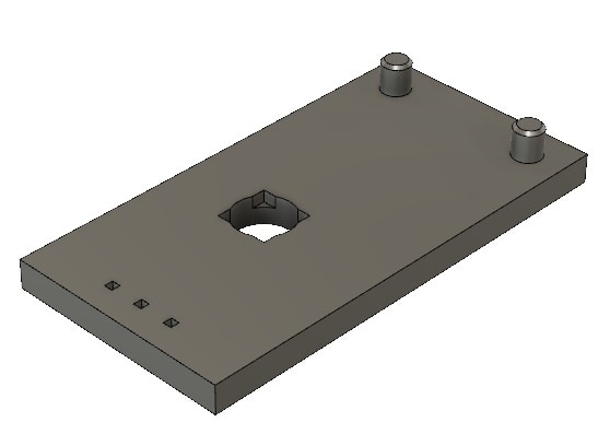
After slicing and then printing my fixture, I did a little cleanup and here is then new soldering jig:
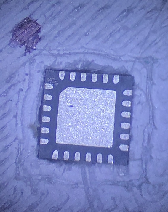
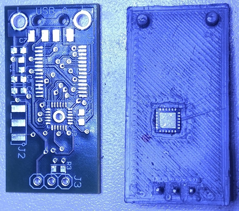
Here is an image of the PCB test loaded into the fixture (chip installed, notice the sharpie mark in the upper left hand corner to remind me of the correct chip position).
Below, we are looking through the through-hole at the exposed pad (the PCB is tilted in the board vise, under the microscope).
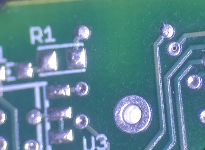
Note: the bright white spot in the center in the center of the pad is the exposed pad of the VQFN24 chip. With the image tilted like this, zooming in allows you to see if the exposed pad is flush with the through-hole pad (now dark shadow, viewed at multiple angles.
With everything looking good, I unmounted the PCB and applied flux to the exposed pad and the top of the through-hole pad and remount the PCB into the soldering jig. I then proceeded to feed solder into the through-hole pad, moving the soldering iron tip around the hole, allowing the solder to bound to the exposed pad. Then after allowing the solder to cool, I carefully removed the PCB from the soldering jig (while pressing on the chip top to free it from the indent). Here are some images of the pin-to-pad alignment:
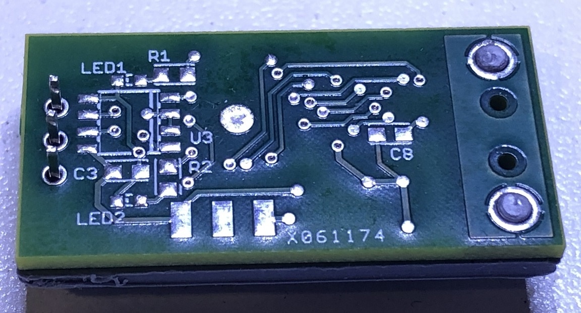
Here is an image of the PCB is soldering jig, after soldering to the exposed pad via the through-hole (the hole is filled, nearly flush to the surface).
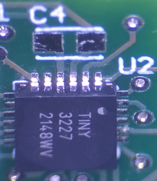
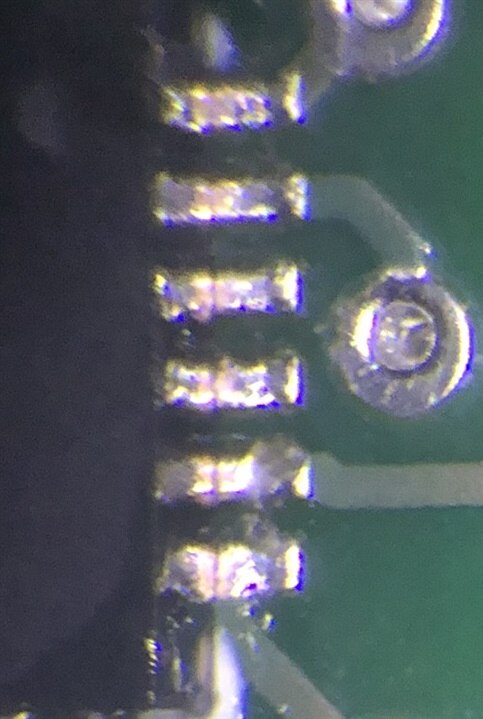
The alignment is very good (notice the longer than normal pads on the PCB, I wanted to be sure to have plenty of pad space to apply heat to while soldering). I also verified that the chip pads were in all equally positioned to the surface of the PCB. From there, I applied solder flux and soldered the pins by placing a small blob of solder on the first pin and carefully dragging across the remaining pins. Some sides required a few drags to get all of the pads soldered, with not solder bridges.
Now, I need to test each of the pins to see if I have continuity and no shorts. I will be saving that task for a while as my coordination and energy levels are a bit impaired. Yesterday I tested positive for COVID after having some cold like symptoms. We had recently traveled, to Tacoma to visit with relatives and I am sure that the while flying (fully masked) with mostly unmasked passengers we were infected. I am doing fine, just tired, fuzzy, coughing and congested. My wife tested negative, so I am isolating in my office and a spare bedroom, although she is pretty sure that she is coming down with it too. Thankfully we are both fully vaccinated and boosted (x2), so this should not be a huge problem.
