

In the first blog of this series there is a schematic which shows the two AP Memory APS6404L Pseudo SRAMs connected to the FPGA.
These can be clocked at a maximum rate of 130MHz, but there are some issues in going that fast – firstly the maximum data burst length is only 32 bytes and secondly the sampling window must be aligned so precisely wit the clock pulse that the manufacturer suggests:
For operating frequencies >84MHz, it is highly recommended to utilize CLK falling edge to sample read data or align sampling clock via data pattern tuning (refer to JEDEC JESD84-B50 for an example).
This sounds like hard work, not ideal for the first step in getting the chips going, so I shall keep my clock to below 84MHz.
The board has a 25MHz oscillator so I shall need to use the PLL to make a faster clock in the FPGA. It turns out that the PLL in the Trion series of FPGAs is a bit limited so the best I can do with a 25Mhz oscillator is a 75MHz internal clock.
Top Level Design
I use Aldec Active-HDL for VHDL/Verilog design and simulation. It’s quite expensive but has advantages over the free or bundled tools. One of them is its nice block diagram editor which I used to make this top-level view of the project.

I find the block diagram view at the top level is much easier to understand than its VHDL (or Verilog) equivalent.
Aldec block diagrams compile to bog standard VHDL (or Verilog):
-------------------------------------------------------------------------------
--
-- Title       :
-- Design      : EFTB
-- Author      :
-- Company     :
--
-------------------------------------------------------------------------------
--
-- File        : C:\Docs\Rabbits\Efinix_EFTB_rtl\Aldec\compile\eftb_top.vhd
-- Generated   : Wed Dec 28 14:43:19 2022
-- From        : C:\Docs\Rabbits\Efinix_EFTB_rtl\Aldec\src\eftb_top.bde
-- By          : Bde2Vhdl ver. 2.6
--
-------------------------------------------------------------------------------
--
-- Description :
--
-------------------------------------------------------------------------------
-- Design unit header --
library IEEE;
use IEEE.std_logic_1164.all;

entity eftb_top is
  port(
       clk75 : in STD_LOGIC;
       pll75_rstn : out STD_LOGIC;
       heartbeat : out STD_LOGIC;
       nres : in STD_LOGIC;
       psr_dat_o : out STD_LOGIC_VECTOR(7 downto 0);
       psr_dat_i : in STD_LOGIC_VECTOR(7 downto 0);
       psr_debug : out STD_LOGIC_VECTOR(7 downto 0);
       psr_nce : out STD_LOGIC;
       psr_clk : out STD_LOGIC;
       psr_out_en : out STD_LOGIC;
       psr_test : in STD_LOGIC;
       dbg_mpx : out STD_LOGIC_VECTOR(7 downto 0);
       pll75_locked : in STD_LOGIC
  );
end eftb_top;

architecture eftb_top of eftb_top is

---- Component declarations -----

component debug_mpx
  port(
       db0 : in STD_LOGIC;
       db1 : in STD_LOGIC;
       db2 : in STD_LOGIC;
       db3 : in STD_LOGIC;
       db4 : in STD_LOGIC;
       db5 : in STD_LOGIC;
       db6 : in STD_LOGIC;
       db7 : in STD_LOGIC;
       dbg_mpx : out STD_LOGIC_VECTOR(7 downto 0)
  );
end component;
component psram_ctrl
  port(
       clk_75 : in STD_LOGIC;
       res_hi : in STD_LOGIC;
       psr_nce : out STD_LOGIC;
       psr_clk : out STD_LOGIC;
       psr_out_en : out STD_LOGIC;
       psr_dat_i : in STD_LOGIC_VECTOR(7 downto 0);
       psr_dat_o : out STD_LOGIC_VECTOR(7 downto 0);
       test : in STD_LOGIC;
       psr_debug : out STD_LOGIC_VECTOR(7 downto 0)
  );
end component;
component sync_reset
  port(
       clk75 : in STD_LOGIC;
       nres : in STD_LOGIC;
       res_hi : out STD_LOGIC;
       res_lo : out STD_LOGIC;
       clk_div_8 : out STD_LOGIC;
       heartbeat : out STD_LOGIC
  );
end component;

----     Constants     -----
constant DANGLING_INPUT_CONSTANT : STD_LOGIC := 'Z';
constant VCC_CONSTANT   : STD_LOGIC := '1';
constant GND_CONSTANT   : STD_LOGIC := '0';

---- Signal declarations used on the diagram ----

signal GND : STD_LOGIC;
signal NET1020 : STD_LOGIC;
signal NET799 : STD_LOGIC;
signal NET807 : STD_LOGIC;
signal res_hi : STD_LOGIC;
signal VCC : STD_LOGIC;

---- Declaration for Dangling input ----
signal Dangling_Input_Signal : STD_LOGIC;

begin

----  Component instantiations  ----

U1 : sync_reset
  port map(
       clk75 => clk75,
       nres => nres,
       res_hi => NET807,
       clk_div_8 => NET799,
       heartbeat => heartbeat
  );

U2 : psram_ctrl
  port map(
       clk_75 => Dangling_Input_Signal,
       res_hi => res_hi,
       psr_nce => psr_nce,
       psr_clk => psr_clk,
       psr_out_en => psr_out_en,
       psr_dat_i => psr_dat_i,
       psr_dat_o => psr_dat_o,
       test => psr_test,
       psr_debug => psr_debug
  );

U3 : debug_mpx
  port map(
       db0 => NET807,
       db1 => NET799,
       db2 => pll75_locked,
       db3 => GND,
       db4 => GND,
       db5 => GND,
       db6 => GND,
       db7 => GND,
       dbg_mpx => dbg_mpx
  );


---- Power , ground assignment ----

GND <= GND_CONSTANT;
VCC <= VCC_CONSTANT;
NET1020 <= VCC;

---- Terminal assignment ----

    -- Output\buffer terminals
	pll75_rstn <= NET1020;


---- Dangling input signal assignment ----

Dangling_Input_Signal <= DANGLING_INPUT_CONSTANT;

end eftb_top;
The psram block doesn’t contain any code yet and there isn’t much in the sync_reset block.
In most FPGA design tools inputs and outputs in the top-level are directly associated with pins on the chip. This is not the case in the Efinix design flow which has a peripheral layer between the top level HDL and the chip. This peripheral layer contains not only IO logic but also the PLLs (and some other things). Efinix call the actual FPGA centre the Core.
It takes a little getting used to but it works quite well.
The Aldec tool produces VHDL files and these need to be added into an Efinix project. It’s worth running the synthesis in Efinity (that’s what Efinix call their design tool), at this stage.
Like most FPGA tools it produces a vast amount of running commentary and a summary.
A lot of the IO pins on the block diagram are never driven or don’t drive anything so they get optimised away by the synthesiser.
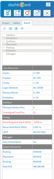
The Efinity Dashboard is telling us that there are a lot of Core pins with nothing to connect to – which is fine because none have been defined yet.
It’s also telling us that the design (what little is left of it) won’t meet timing. That doesn’t matter either – because Efinity assumes a 1Ghz clock if you don’t tell it anything else and we haven’t.
It does tell us that there are no serious errors so we can get on with defining the peripheral stuff.
Peripheral Layer Design
This is where the Efinity approach differs most from other FPGA vendors. Defining pins is always a bit of a mess and this alternative way of doing it might well be an improvement.
First you need to open the Interface Designer.
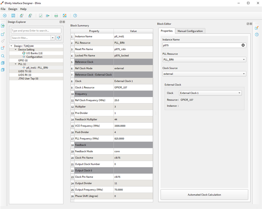
We’ll start with setting up the PLL. Since the 25MHz oscillator on the dev board is already connected to a particular clock input pin we must select a PLL which can use that pin and make sure it is correctly selected.
If you don’t want to use the default names, then you need to enter new ones.
Now we can use the PLL automatic clock tool by clicking the lower button in the right-hand tab.
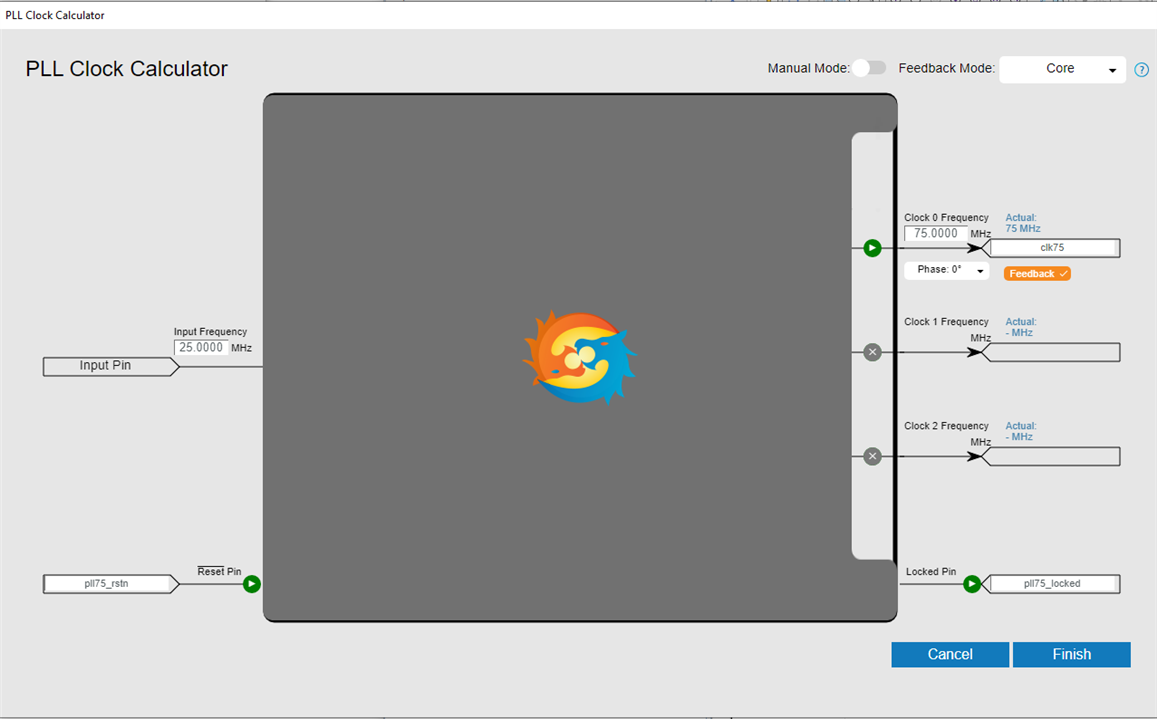
It’s quite simple to use. If you want to mess with the details, you can define all the PLL controls manually but for a single and simple clock that isn’t necessary.
After the PLL we define the GPIOs.
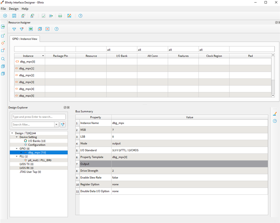
You click on things in the Design Explorer to add or delete GPIO features (like blocks for single pins or buses for groups of pins).
In the screenshot I’m setting up an 8-bit output port. Once the general features are sorted you must define the actual pins used in the top tab.
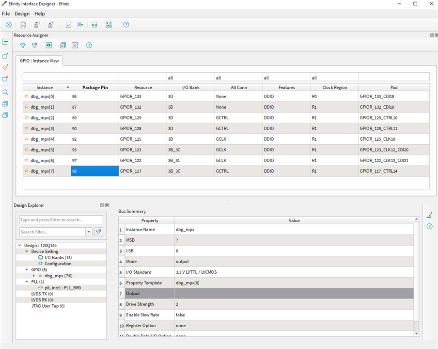
When you think you are done there is a useful check feature which will pick up[ most errors in the Interface design. (But not discrepancies between the Interface Design and the Core design.)
Once it all looks good at this level you can return to the main window and re-run the design.
But actually it’s a good idea to make a start on the constraints file so the built in static timing analysis (which is how you know the design might actually work) can run.
At this stage a really simple set of constraints will do.
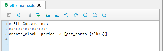
All it does is tell the timing analyser how fast the clock is.
When we re-run the tool we get this:

There is still one unassigned core pin. From the diagnostic output I know that it’s the output enable for the IO port.
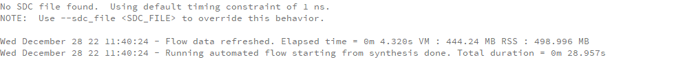
I suspect its to do with so much of the IO being optimised away but I won’t know until I add a bit more to the design.
The Dashboard is also telling us that we could increase the 75MHz clock to 226MHz, but this isn’t very realistic because so little of the design is in place.
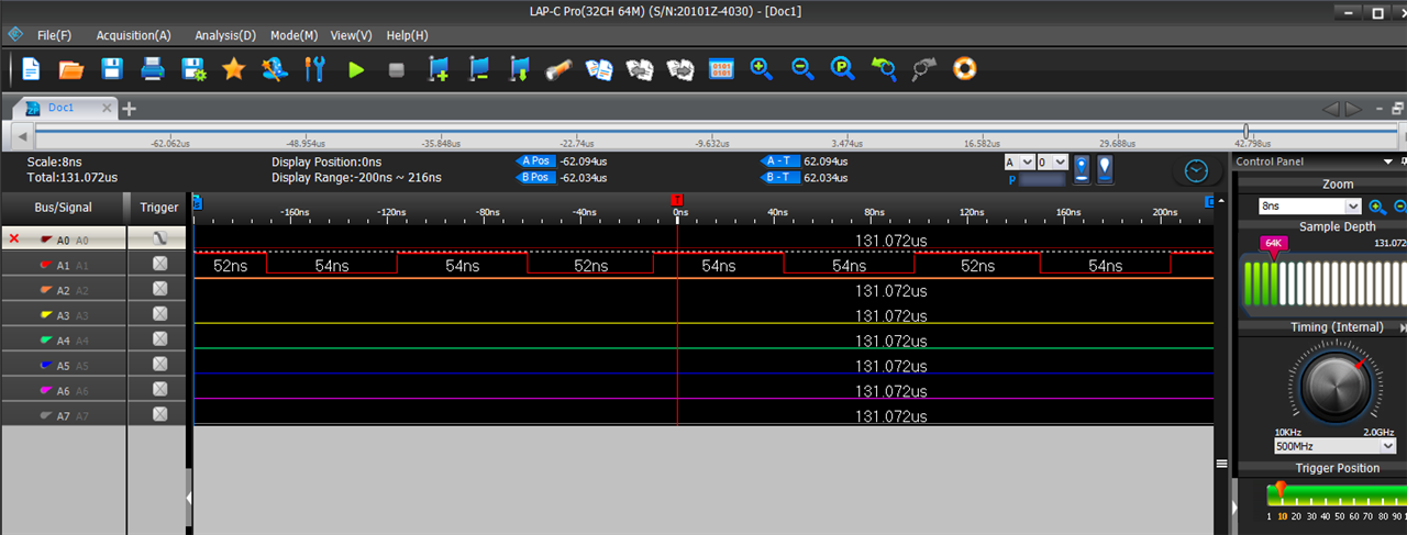
It runs as it is, and the logic analyser can show us the 75MHz clock divided by 8.
So that's a very basic project set up in Efinity with some IO and a PLL. The next step is to do some real code to work the memory chips.
MK
-

dougw
-
Cancel
-
Vote Up
0
Vote Down
-
-
Sign in to reply
-
More
-
Cancel
Comment-

dougw
-
Cancel
-
Vote Up
0
Vote Down
-
-
Sign in to reply
-
More
-
Cancel
Children