The first part of this project kicked off with a blog “First Design with KiCad (8.0)” about 4 weeks ago. The idea was to build a replacement for obsolete TO3 can linear voltage regulators using the Linear Technologies (now owned by Analog Devices) LT8640s low noise switching regulator.
This was my first KiCad project and the pcb design went quite well.
The boards came from PCBCart in China and I had no issues with them working with the KiCad Gerber and other outputs.
Because the board is an odd shape I had it made in a 1 x 1 panel.
Here are 4 with the solder paste screened on and some of the parts placed.
And here they are again after solder reflow.
There were two errors in the design. Both were my fault
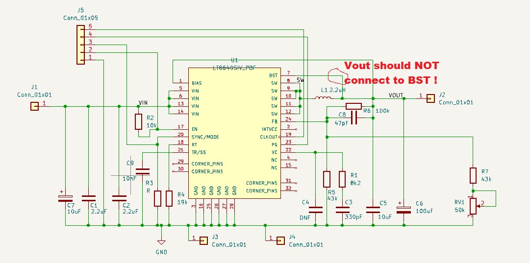
For some reason I connected BST to the output. I can’t think why because the data sheet says:

To save anyone else the trouble of trying it – don’t - it doesn’t work !
Easily fixed by cutting a track.
The second error was that I made the holes for the two press fit pins too large (Mill-Max 8979-0-00-15-00-00-03-0 from Mouser)
I specified a 1.9mm hole, which is bigger than the pin data sheet says – I should have gone smaller and opened it out if necessary. Not the end of the world, I squeezed the heads of the pins which gave them some grip and then soldered them.
Testing
I tested the board without any heat sinking.
I used a pair of Keysight 34465A DMMs to measure input voltage and current. Power was supplied by an AimTTi QL564TP power supply but its readout isn’t terribly accurate. I trusted the Rigol DL3031A active load to measure load voltage and current. It was connected with Kelvin leads using the remote voltage sense capability which would have worked better if I had turned it on !
I was in a hurry to get data so I didn’t automate the measuring but entered it by hand into Excel.
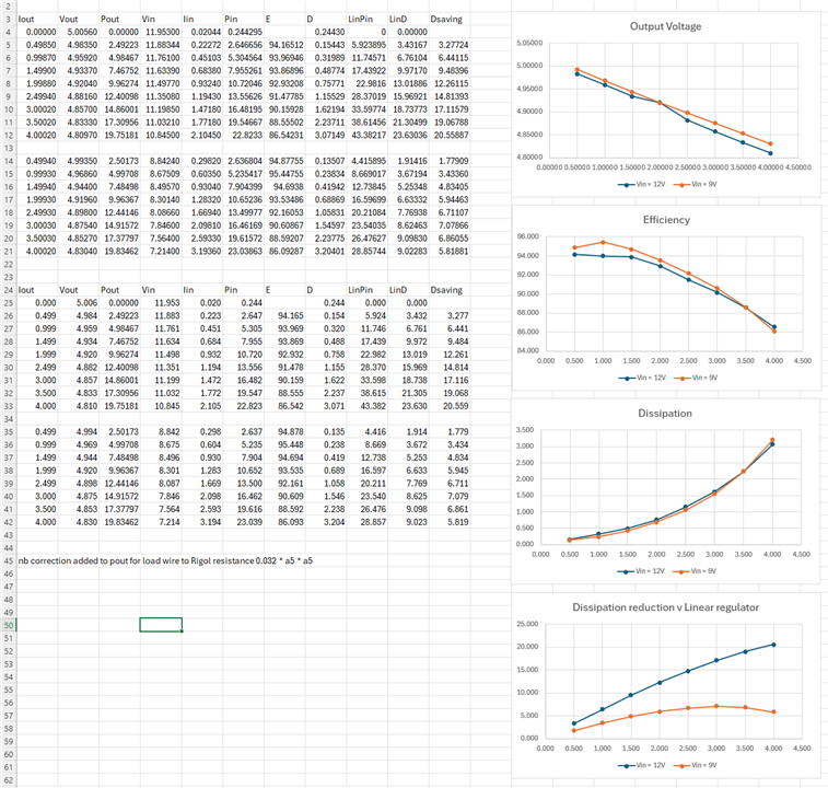
The first block of data from lines 3 to 21 is the measured values:
Vout, Iout, Vin and Iin (that’s I in )
The computed values are:
Power out, Power in, E (efficiency), D (dissipation), LinPin (the input power if it had been a linear regulator), LinD (dissipation if it had been a linear regulator) Dsaving (reduction in power input by using a switcher).
The second block of data (lines 24 to 42) is a copy of the first but rounded to three decimals.

And then that note !
Looking at Vout (2nd col, lines 4 – 12) the voltage regulation is a bit disappointing. This was because the remote voltage sense on the Rigol load was not turned on (it defaults to off on power up and can’t be made to save the previous state). So the voltage drop along the quite long wires to the Rigol is causing an error. Rather than repeat all the measurements I added a compensation factor to the output power, using this formula for the Pout col:
=A5*B5 + (0.032 * A5 * A5)
So I have added the power lost in the wires to the output power calculated by multiplying the voltage and current as measured by the Rigol load. The resistance of the wires is 0.032R which I measured by comparing the voltage measured by the Rigol with remote sensing turned off and then on.
The output voltage graph is wrong because of this error – it should show a drop of about 40mV at 4A rather than about 180mV (0.8% rather than 3.6%).
The other three graphs are correct and show that the efficiency remains above 90% for output currents up to 3A.
At 4A output the board is getting quite warm and the rise of the case temperature of the LT8640s above ambient is about 55K. I’ll experiment with a heatsink later.
I’ve tried to show the benefit of using the switcher compared with a linear regulator. The data with a nominal 12V input represents a reasonable design if a simple transformer, rectifier and smoothing capacitor type power supply is used to provide the input power. The approx 1V drop caused by the wires in my test setup is not far from what might be expected from an unregulated supply.
So at 3A load current the switcher reduces the heat dumped into the rest of the system by 20W.
I did some quick noise and transient response measurements.
The Rigol load can do pulsing so I set it up to pulse the current from 1A to 3A for 50ms with a current slew rate of 0.5A/us.
The response transients for load current rising or falling a very similar. They should be treated with caution because active loads have their own transient difficulties and I have not yet checked the Rigol DL3031A transient behaviour.


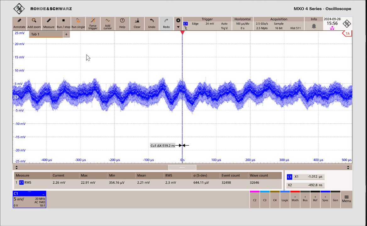
The output noise at 1A load current looks OK at 10mV pk-pk

I’m not totally convinced by the noise (it was measured hastily). Looking with a slower time base shows the nose envelope with some very unexplained modulation at low 10s of kHz frequencies – looks a bit like AM radio !

The noise with the scope probe connected to the ground terminal shows unexplained little spikes at about 20kHz repetition rate – I don’t think the LT8640 is making these, but more work is required to be sure.

Summary
This first quick look at the performance of my TO3 shaped LT8840s Silent Switcher board shows that it works fairly well.
It can deliver 3A safely (and 4 at a pinch) with no heat sinking and has acceptable regulation, noise and transient performance.
As you would expect from a switcher it saves a lot of power but this comes at a very high financial cost – the BOM cost of this design is about £21 (allowing £5 each for pcbs). To compare the sublime with the ridiculous, I just bought 20 L7805CV TO220 5V regulators from Amazon – sourced from “BOJACK” for £7.88 (£0.39 each) – they won’t manage 3A and I have no idea who made them. A good ST 7805 in an insulated TO220 package costs about £1.
I’m thinking of building a much better test rig for small PSUs. When measuring efficiency we need to compare power in to power out and with good regulators we may be interested in measuring efficiency above 95% and would like better than 0.1% accuracy of the efficiency measurement.
This implies that the voltages and currents should be measured to (quite a lot) better than 0.01% accuracy.
There are very few (if any) bench top DMMs capable measuring 10A DC that accurately. I have a cunning plan but that’ll need to wait for another blog.
MK

-

jc2048
-
Cancel
-
Vote Up
0
Vote Down
-
-
Sign in to reply
-
More
-
Cancel
-

dougw
in reply to jc2048
-
Cancel
-
Vote Up
0
Vote Down
-
-
Sign in to reply
-
More
-
Cancel
Comment-

dougw
in reply to jc2048
-
Cancel
-
Vote Up
0
Vote Down
-
-
Sign in to reply
-
More
-
Cancel
Children