element14 Community
element14 Community
    Register Log In
  • Site
  • Search
  • Log In Register
  • About Us
  • Community Hub
    Community Hub
    • What's New on element14
    • Feedback and Support
    • Benefits of Membership
    • Personal Blogs
    • Members Area
    • Achievement Levels
  • Learn
    Learn
    • Ask an Expert
    • eBooks
    • element14 presents
    • Learning Center
    • Tech Spotlight
    • STEM Academy
    • Webinars, Training and Events
    • Learning Groups
  • Technologies
    Technologies
    • 3D Printing
    • FPGA
    • Industrial Automation
    • Internet of Things
    • Power & Energy
    • Sensors
    • Technology Groups
  • Challenges & Projects
    Challenges & Projects
    • Design Challenges
    • element14 presents Projects
    • Project14
    • Arduino Projects
    • Raspberry Pi Projects
    • Project Groups
  • Products
    Products
    • Arduino
    • Avnet Boards Community
    • Dev Tools
    • Manufacturers
    • Multicomp Pro
    • Product Groups
    • Raspberry Pi
    • RoadTests & Reviews
  • Store
    Store
    • Visit Your Store
    • Choose another store...
      • Europe
      •  Austria (German)
      •  Belgium (Dutch, French)
      •  Bulgaria (Bulgarian)
      •  Czech Republic (Czech)
      •  Denmark (Danish)
      •  Estonia (Estonian)
      •  Finland (Finnish)
      •  France (French)
      •  Germany (German)
      •  Hungary (Hungarian)
      •  Ireland
      •  Israel
      •  Italy (Italian)
      •  Latvia (Latvian)
      •  
      •  Lithuania (Lithuanian)
      •  Netherlands (Dutch)
      •  Norway (Norwegian)
      •  Poland (Polish)
      •  Portugal (Portuguese)
      •  Romania (Romanian)
      •  Russia (Russian)
      •  Slovakia (Slovak)
      •  Slovenia (Slovenian)
      •  Spain (Spanish)
      •  Sweden (Swedish)
      •  Switzerland(German, French)
      •  Turkey (Turkish)
      •  United Kingdom
      • Asia Pacific
      •  Australia
      •  China
      •  Hong Kong
      •  India
      •  Korea (Korean)
      •  Malaysia
      •  New Zealand
      •  Philippines
      •  Singapore
      •  Taiwan
      •  Thailand (Thai)
      • Americas
      •  Brazil (Portuguese)
      •  Canada
      •  Mexico (Spanish)
      •  United States
      Can't find the country/region you're looking for? Visit our export site or find a local distributor.
  • Translate
  • Profile
  • Settings
Arduino
  • Products
  • More
Arduino
Arduino Forum Reverse Engineering old serial devices and cloning with arduino.
  • Blog
  • Forum
  • Documents
  • Quiz
  • Events
  • Polls
  • Files
  • Members
  • Mentions
  • Sub-Groups
  • Tags
  • More
  • Cancel
  • New
Join Arduino to participate - click to join for free!
Actions
  • Share
  • More
  • Cancel
Forum Thread Details
  • State Suggested Answer
  • Replies 10 replies
  • Answers 2 answers
  • Subscribers 391 subscribers
  • Views 1089 views
  • Users 0 members are here
Related

Reverse Engineering old serial devices and cloning with arduino.

Former Member
Former Member over 11 years ago

I guess this is a strange topic and might not be one anyone here could give any advice on but here goes...


I have a piece of music equipment that uses a remote control. This remote control communicates bi-directionally with the main unit.

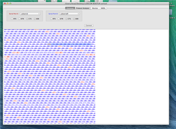
It communicates over RS-422 protocol (mainly for the cable distance, i believe)


I have purchased a couple of rs422 to usb adaptors with the intention of snooping the data in both directions using some serial port monitoring software.

I havent quite gotten that to work properly on its own yet I think its most likely the connection settings I am attempting as the data I see looks messed up.

From what I can tell from the service manual this should be 8 Bit Characters with no parity and 2 stop bits.


Anyways, as this device is now archaic in terms of technology (1982, I believe) i think it would be a great candidate for cloning with an arduino.


The remote itself uses an old intel 8749 microcontroller. this was an MCS-48 based device (i think) which also had a small eprom built into it for program memory.

this was 8-bit with 3 I/O ports.


The remote unit basically has 12 old litronics DL-1414 alphanumeric 4 digit displays (which recieve an ascii character and hold it in their memory until refreshed), a bank of buttons and faders (which are conected via an adc) and a db level meter.


I have the service manual of the unit which goes into much more depth about the bit addressing scheme of the devices. Which I can upload.


I might be thinking about this the wrong way but my idea was to sniff and capture the data being sent and recieved to figure out what is sent, when for instance, a fader is moved. This I would imagine would then be easy to strap to a slide pot in arduino and then have that movement sent to the serial bus possibly with some control bits added and then the value.


I'd really appreciate some thoughts and maybe advice on how such reverse engineering can be tackled...


Thanks in advance,

Brad

  • Sign in to reply
  • Cancel

Top Replies

  • michaelkellett
    michaelkellett over 11 years ago +1 suggested
    USB adapters aren't the best way to do this (but might be your only choice). A logic analyser or better still a scope and a logic analyser (built in or separate) are the ideal tools. You can use the scope…
  • michaelkellett
    0 michaelkellett over 11 years ago

    USB adapters aren't the best way to do this (but might be your only choice). A logic analyser or better still a scope and  a logic analyser (built in or separate) are the ideal tools.


    You can use the scope to check baud rate, data bits and parity etc that is actually used (never trust a manual 100%) and the packet structure of the data.. The logic analyser needs to be able to decode the serial stream and then you can look at the actual data in the packets.


    There are some very cheap logic analysers on the market that will do the job.


    If you are stuck with your 422->USB converters then make sure they are set up for least possible buffering and quickest response (otherwise they may mess up the packet structure). What software are you using to look at the data  - it is quite unlikely to be ascii coded.


    MK

    • Cancel
    • Vote Up +1 Vote Down
    • Sign in to reply
    • Verify Answer
    • Reject Answer
    • Cancel
  • Former Member
    0 Former Member over 11 years ago in reply to michaelkellett

    HI Michael,

    thanks for your response.

    I do have a scope, but its pretty archaic. just an old 20mhz Goldstar thing I picked up.

    I've been looking around at these logic analyzers. the USBEE thing looks kinda cool and only around $50.

    Some of the reason it seems i might be reading garbled data is that I might be probing the wrong lines. I've split open a cable and then spliced into it again.

    The cable of course is RS422 but also carried 11VAC to power the remote. Its possible that the data is 'inverted' from what I'm looking at.

    I was thinking of getting a couple of those little rs422 > rs232 convertor plugs first (since I can use a psu to directly power the remote unit) so that rather than mess and guess with 4 comms wires I'm only messing with 2. to make it a bit more fool proof.


    I have OCR'd a few of the important pages in the service manual, I'll paste it here... it seems like I should be able to get a good deal of info from it, but I'm still a little in the dark as to how i would actually structure data coming out of the arduino.. perhaps if you have any time to read a bit of it , you can maybe give me some starter points?


    here goes:


    1. 4.7.1 Power Supply


    The power supply for the REMOTE is a 5V switching regulator- The central item in this regulator is an MC34060 or TI 494 pulse width modulation (PWM) control chip. The 34060 produces an output control whose duty cycle multiplied by the input voltage is equal to 5V. This control is then applied to a pass transistor (01) located between the input voltage and an output filter. The output filter is a low-pass filter with a single pole at a frequency sufficiently low to attenuate the switching frequency and harmonic components in the switched square wave. 


    The input section is relatively simple. The REMOTE may be powered from one of two sources; from the mainframe through Jl, or from an alternate power source through J2. Note that whenever a plug is inserted into J2, an integral switch disconnects the mainframe power source. C30, and FB3-4 form a simple RF filter for the mainframe power source; C23 and R13 provide a bypass for RF and static between the cable shield and REMOTE ground; and C31-33 and FB5-8 form a two stage RF filter for the alternate power source.
    The CR7 bridge rectifier is provided so that either AC or DC power may be used (the mainframe power is rectified).C35-37 form a composite filter capacitor operating over a large frequency range with low ESR. F1 was chosen through extensive testing to be a 1 amp fast fuse. Note, however, that one fault condition can occur that can not be protected by this (or any other) fuse: when the REMOTE is being powered by the mainframe, the fuse will not blow if a short occurs in the IARC circuitry after the regulator, because the mainframe can not provide enough power to blow the fuse. This fault condition will not damage the regulator or the mainframe.


    The 34060 accepts a Vcc input (pin 12) from which the chip is powered and a 5 V reference (Vref, pin 14) is produced. This Vcc may be from 7 to 40 Vdc, and need not be carefully regulated. The dead time input (DT, pin4) is used to "soft start" the regulator; when DT Is near
    Vref the regulator is effectively shut down, and when DT is near ground the regulator is allowed to function normally. Thus as C39 is charged from Vref through R19 and R20, the output of the power supply ramps up from 0V to the normal 5V output.
    The 34060 generates the switching frequency internally using the external timing components RT (pin 6 connected to R21) and CT (pin 5 connected to C40). The switching frequency is 1.1/(RT*CT) , which figures out to approximately 50 kHz in the REMOTE. The output transistor of the 34060 is controlled by the product of comparators whose inputs are an internal ramp waveform at the switching frequency, the dead time input, and the sum of two other comparators whose inputs are pins 1 and 2, and 16 and15. The first comparator is used to compare the regulator output voltage with the reference voltage. The second comparator (which is normally used for current limiting) is not used, and its inputs are tied off. The COMP input (pin 3) is used for compensation of the comparators. The output transistor is used common-emitter fashion to control the pass transistor.


    The output section of the regulator consists of the pass transistor (a P-channel MOSFET) and output filter (a single pole LC low-pass filter). The pass transistor is tumed on when its gate is pulled to ground by the output transistor of the 34060. R22 is used to quickly dis-charge the pass transistors stray gate capacitance when the 34060 output transistor turns off" The output of the pass transistor is a 50 klfz square wave which swings from ground to the input voltage and whose average voltage is 5 V. The output filter (which consists of CR8, FB 9 and 10, L1, and composite capacitor C41 and C42) has its pole at 83 Hz and is used to block the 50 Khz (and higher harmonic) components of the square wave, yielding only the DC component at the output (the desired 5 VDC).


    1. 4.7.2 CPU


    The central processing unit of the REMOTE is an 8749, containing the CPU, clock oscillator, RAM, UV eras-able ROM, and three 8-bit I/O ports on a single chip.


    The XTAL 1 and XTAL 2 (pins 2 and 3) are connected to a 4.608 MHz crystal, yielding a processor throughput of 307,200 instruction cycles/second. The ALE output (pin 11) is a 20% duty cycle square wave at the same frequency as instruction cycles (307.2 kHz), and is present whenever the 8749 has power. This the first place to verify that the processors clock is correctly functioning.


    The three I/O ports are used as follows: The BUS port (pins 12-19) is used as a bidirectional data bus. It is used in two modes; in the tristate mode to transfer 8-bit data to the Litronix DL-1414 intelligent displays from the ADC0809 A/D converter, and both to and from the CDP1854 UART; and in the latched mode (through the NE594 buffer/driver) to scan the switches and head- room LEDs. Bits 0-6 of Port 2 are outputs used as the address bus bits A0-A6, and bit 7 is used as the FSK tape output. Bits 0-3 of Port 1 are used as inputs from the switch array (B0-B3), and bits 4-7 are used as outputs controlling which section/row is lit in the head-room LED array (S0-S3)


    There are also several control pins on the 8749: the SS input (pin 5), which must be unconnected for correct operation; the EA input (pin 7), which must be grounded for correct operation; the INT/ input (pin 6), which the UART pulls low to signal the processor when a character is available; the T0 input (pin 1), which the processor can read to determine if there was a framing error on the last character received (this feature is not currently used by the software); the T1 input (pin 39), which the processor reads during FSK tape input; the PROG/ output (pin 25), which is normally used with a 8243 I/O port expander, but is used in the REMOTE to clock the address of the slider to convert into the ADC0809; and the RD, WR and PSEN (pins 8, 9, and 10) outputs, which are normally used for external memory access, but are not used in the REMOTE.


    1. 4.7.3 Reset Logic


    Both the 8749 and the CDP1854 need to be reset after power up. A simple RC (R7 and C9) circuit is used as an input to a differential driver (U3, the uA9638) to pro- duce the required RES and RES/ signals, which are asserted for approximately 1/4 second after power is applied. The CR5 Schottky diode is used to quickly discharge C9 when power is removed (or when power is momentarily lost). To manually reset the REMOTE momentarily ground pin 3 of US.


    1. 4.7A Address Decoding Logic


    In order to be able to access the devices that share the data bus (the ADC0809, CDP1854, and 12 DL-1414s), an address decoder is used. Address bits A2-A5 are decoded into 16 low-active chip select lines using a CD4515 4-to-16 line decoder. Address bit A6 is used as the decoder enable so that any race conditions (which may cause glitches in the decoder outputs) are eliminated.


    When addressing devices, the software in the 8749 goes through several steps to assure that the addressing is done without any glitches. When addressing devices for output (such as the CDP1854 and DL-1414s), the 8749 first places the output data on the BUS port, presents the address of the desired device on A0-A5, then pulls A6 low to address the device, and lastly pull A6 high again to disable the device. When addressing devices for input (such as the CDP1854 and ADC0809), the 8749 first tristates the BUS port, presents the address of the desired device on A0-A5, pulls A6 low to address the device, then reads the desired input data from the BUS port, and lastly pulls A6 high again to disable the device.


    A simple device address map is show in in Table 4.24


    Device AS A4 AS A2 Al AO


    DL-1414, Ul, Display Bd 0 0 0 0 C C
    DL-1414, U2, Display Bd 0 0 0 1 C C
    DL-1414, US, Display Bd 0 0 1 O C C

    1. DL-1414, U4, Display Bd 0 O 1 1 C C
    2. DL-1414, US, Display Bd 0 1 0 0 C C
    3. DL-1414, U6, Display Bd 0 1 0 1 C C
    4. DL-1414, Ul, Paneled 0 1 1 0 C C
    5. DL-1414, U2, Panel Bd 0 1 1 1 C C
    6. DL-1414, US, Panel Bd 1 0 0 0 C C
    7. DL-1414, U4, Panel Bd 1 0 O 1 C C
    8. DL-1414, US, Panel Bd 1 0 1 0 C C
    9. DL-1414, US, Panel Bd 1 0 1 1 C C
    10. CDP18S4 character output 1 1 0 0 X X
    11. CDP18S4 character input 1 1 0 1 X X


    1.  
    2.  


    Where: XX are don’t cares, and CC is the code for the character within a DL-1414 display chip: 00 is the right-most character, 01 is the second from the right, 10 is the second from the left, and 11 is the left-most character.


    1. 4.7.5 ADC Logic


    The first item of interest concerning the ADC0809 is its power source; in order to guarantee that any switching supply noise will not affect the converter, a filter is used between the 5 V supply and the ADC0809s Vcc input. The finer is an RC finer consisting of R12 and the composite capacitor C16 and C17. Since the ADC0809 is CMOS (and consequently low power), the voltage drop across R17 is minimal. Note also that all the analog inputs are decoupled for further noise immunity.


    Parts of the addressing logic for the ADC0809 are slightly more complicated than the other chips on the data bus. The ADC0809's internal analog multiplexer address (the address of the slider to convert) is transferred to the ADC0809using the 8749s PROG/ output, which is normally used with 8243 Port 2 expander chips. When the processor wishes to change the address of the slider to convert, it uses a command which places a flurry of (mostly useless) information on A0-A5. During this command, the address of the slider to convert is placed on AO-A5 400 ns before the rising edge of PROG/, and is held for 90ns after the rising edge.


    After the processor sets up the address of the next slider to convert, the processor will read the results of the last conversion and start the next conversion simultaneously by addressing the ADC0809 for input as described in section 4. Note that the ADC0809's end of conversion (EOC) output is not used since the processor s software never accesses the ADC0809 more often than the 250 microsecond conversion time.


    The last item of interest concerning the ADC0809 is the circuitry associated with analog inputs INS and IN7, which is used to measure the 5 V power supply's actual voltage. The circuit-connected to lN6 is a resistor/zener diode constant voltage source (RIO and CR6). The digital code resulting from the conversion of this signal will change as the supply voltage to the ADC0809 changes, because the ratio of the supply voltage to the constant voltage will change The circuit connected to IN7 is simply a resistive voltage divider (R9 and Rll) with an adjustable output voltage. Since the voltage source to this divider is the same as the ADC0809 supply voltage, the resulting digital code from the conversion of this signal will be always a constant. If the adjustable voltage source is adjusted so that it is the same as the constant voltage source when the S V power supply is at 5.00 V, then the actual voltage of the S V power supply is calculated using a linearization of the system equations governing these circuits.


    1. 4.7.6 UART Logic


    The UART data is read and written using the addressing scheme in section 4. The UART clock inputs (RCLK and TCLK pins 17 and 40), which are 16 times the 9600 baud data rate, are derived by dividing the 307.2 kHz ALE clock by two using 1/2 of the CD4O1S flip-flop. The UART is strapped to provide and recognize 8-bff characters with no parity and 2 stop bus. The UART data available (DA, pin 19) output, which signals that the UART has received a complete character, is inverted before being used to interrupt the processor.


    1. 4.7.7 RS-422 Logic


    The serial data to and from the UART is converted to RS-422 compatible signals by the uA9SS7 (U2) differential receiver and the uA96S8 (US) differential driver.The LC filter comprised of C27, FBI and FB2 is used to rate limit the signal rise and fall times (and thereby reduce RF noise), and the R14 termination resistor is used to eliminate signal reflections.


    1. 4.7.8 Lltronlx Display Logic


    The Litronix DL-1414 displays act very much like as a memory device that happens to display its memory's contents. Once a character has been written to the DL-1414, it will be displayed without any need for refresh from the processor. When the addressing scheme from section 4 is used to output data to the DL-1414, the data on the BUS port is the character to display (in ASCII), the AO and Al lines correspond to the character to display within a given display chip, and the A2-A5 lines correspond to the address of the display chip. Remember that these lines are decoded by the CD4515 into low-going enable lines, which are connected to the WR/ (pin 3) lines of the DL-14148 and used to clock the data into the displays. Remember that the characters within a chip are numbered from character 00 on the right to character 11 on the left.


    1. 4.7.10 Buffered Bus and Sink logic


    The NE594 driver circuit buffers the BUS port and provides current drive capability for the headroom LEDs. No headroom LEDs, however, will light unless the appropriate current sink (the 75492, U4) is activated also. Therefore when the processor is using the data bus to communicate with the DL-14148,
    ADC0809, or the CDP1854, it keeps the sinks deactivated so that the LEDs do not light up spuriously. Upon reset of the 8749, all the bus on Port 1 and Port 2 are set to logic 1; therefore Port 1 bus 4-7 are inverted before the 75492 so the LEDs do not light up during power up. R5-R12 on the Panel board are provided for LED current limning.


    The Panel board switches are also scanned from the NE594 buffered BUS output. CRI-CR8 of the Panel board are provided so that "sneak paths” will not cause the LEDs to light if multiple buttons are pushed. R1-R4 of the Panel board provide a pulldown to ground, which is the default condition when buttons are not pushed.


    The REMOTE processor software does not scan its LEDs and switches simultaneously. The software first will scan the LEDs, lighting eight at a time:the data for each group is placed on the BUS port, then the appropriate bit on Port 1 is set low for several hundred microseconds, then it is set high again. After all the LEDs have been scanned, then the processor will scan all the switches, scanning four at a time: the appropriate bit for each group on the BUS port is set high, then the processor reads the BO-83 bits from Port 1 to determine the states of the buttons in the selected column. Note that the processor scans only the switches during the Diagnostic Menu Mode; the LEDs are not scanned.

    • Cancel
    • Vote Up 0 Vote Down
    • Sign in to reply
    • Verify Answer
    • Cancel
  • michaelkellett
    0 michaelkellett over 11 years ago in reply to Former Member

    It is an ancient device !

    I can't think how long it is since I used on off processor UART !


    There are a few ways you could get wires crossed (literally).

    Since you ultimately want to use the Arduino you will need an RS422 transceiver at some point. Do you have a solution for this.

    If not you can buy boards (shields) or if you can mange a chip and veroboard you can buy a TI DS3695N for about £1.


    Once you have RS422 - 5V logic level you can connect up to the Arduino - but you can also monitor the data on your scope. It will then be easy to tell if the connections to the RS422 are the right way round.


    MK


    • Cancel
    • Vote Up 0 Vote Down
    • Sign in to reply
    • Verify Answer
    • Cancel
  • Former Member
    0 Former Member over 11 years ago in reply to michaelkellett

    I thought it would be more prudent to try to get somewhere without the arduino first, just by using some software to sniff the streams and then see what I can send back to get some responses?


    Are you suggesting to go straight to arduino?

    • Cancel
    • Vote Up 0 Vote Down
    • Sign in to reply
    • Verify Answer
    • Cancel
  • michaelkellett
    0 michaelkellett over 11 years ago in reply to Former Member

    The problem you have is that the Arduino serial ports work at 5V logic level and  a PC will probably only have USB. So you end up needing different [RS422 -> something] converters. USB to serial adapters can often add their own issues.


    Since you already have the RS422 -> USB converters we may as well start with them:

    You need to get your scope on the RS422 wires so you can sort out what's going on.

    What make/model are the RS422 converters, what software are you running on the PC to talk to them (if at all possible please try using Hyperterminal - it's much simpler than many of the alternatives and so easier to debug.)

    Do the two RS422 adapters appear as different COM ports ?


    The  basic plan is to use your scope to look at signals on RS422 being sent from the PC first - then we know what the PC expects to receive. Then you can check the signals from the remote and make sure that they are the same format and polarity as the PC is sending out. At this point it ought to work.


    MK

    • Cancel
    • Vote Up 0 Vote Down
    • Sign in to reply
    • Verify Answer
    • Reject Answer
    • Cancel
  • Former Member
    0 Former Member over 11 years ago in reply to michaelkellett

    HI Michael,

    Firstly, thank you for your responses, they are certainly helping to steer me down the right path.


    In terms of using my scope to ascertain the signal, It's a really old Goldstar unit, analogue 20mhz, and I'm not super skilled at using it yet.. I was able to find pulses with it though when pressing buttons.


    I cant remember the make of the USB adaptors, but, (I think) i had some success this evening with more tinkering..


    I cut the serial cable in the middle and soldered both ends to a vero board with some headers in between, attached the usb convertor and started seeing a data stream.

    I started to build a map of what data was sent when moving controls and pressing buttons on the remote and, because of some of the data I read I believe that I must have the correct settings..


    Moving the faders on the unit in succession I see this:


    FADER 1

    <C0> - <value from 00 to FE>

    FADER 2

    <C1> - <value from 00 to FE>

    FADER 3

    <C2> <value from 00 to FE>

    and so on...


    When Fader 1 is moved it sends <C0><00><C0><01> etc etc all the way to <FE> I believe this is 0-255 so because that makes sense and is coherent should I assume I'm getting valid data?


    Now, the host (not a pc, a rack unit controlled by an old 70s single board computer) sends back data when it recieves these commands.

    I'm expecting this to be packets to update the Litronix displays etc. however, I havent been able to pull any ascii characters out of the reponses, which in teh service manual says each one of those displays accepts an hex ASCII value to display the char.

    Additionally after a few seconds the host sends another flurry of data at which time the displays update to display the previous characters before a control was moved.


    using hyperterminal, I wasnt able to get any intelligble characters, only loads of diamonds, ampersands and smilly faces. alll strange ascii characters.


    I resorted to a serial port monitor program on mac to get the above results.


    Am I on the right path?

    I guess I need to figure out these responses next?

    • Cancel
    • Vote Up 0 Vote Down
    • Sign in to reply
    • Verify Answer
    • Cancel
  • Former Member
    0 Former Member over 11 years ago

    Also, forgot to mention, I also recorded the bi-directional data using both usb adaptors.

    That the host was sending on one and what the remote was sending on the other.
    In the screen shot attached, you can see that at idle, the remote (displayed in red) site there constantly spitting out <CC> while the host replies in BLUE (with 30 bytes??) with a repeating response until a parameter is changed.

    You can see from this where I got my results...


    image

    • Cancel
    • Vote Up 0 Vote Down
    • Sign in to reply
    • Verify Answer
    • Cancel
  • michaelkellett
    0 michaelkellett over 11 years ago in reply to Former Member

    It looks as if you are on your way - if I were you the next thing I would do is to write my own program to run on MAC or PC to present and log the data (unless you can configure the terminal prog to do this). It would be much easier to understand if it's presented in packets the way the devices send it and then as you start to understand it you can add decoding features to your prog. I would would use the original Visual Basic (VB6) to do this but no doubt others would use something written in this century.


    MK

    • Cancel
    • Vote Up 0 Vote Down
    • Sign in to reply
    • Verify Answer
    • Cancel
  • Former Member
    0 Former Member over 11 years ago in reply to michaelkellett

    Thanks MIchael,

    I'm also having a lot of fun trying to figure it out.

    I don't really posess the skills right now to go creating a program to 'present and log" the data.

    Would you mind ellaborating a little further on the purpose of this? If push came to shove, I'd employ the services of someone capable of doing this for me perhaps.

    • Cancel
    • Vote Up 0 Vote Down
    • Sign in to reply
    • Verify Answer
    • Cancel
  • Former Member
    0 Former Member over 11 years ago

    thank you very much for all your help Michael,

    You were right about the manual not always being right.

    After messing (for many hours) I found that the data was in fact 7 bits. as soon as I switched this, I started seeing much better data. ASCII characters etc..

    From this I have now been able to make a map of off the comands the remote sends and observed how the responses come back to the remote for the lcd displays.


    I'm going to start a new thread now to ask questions about the next phase I am looking at...


    thanks again

    • Cancel
    • Vote Up 0 Vote Down
    • Sign in to reply
    • Verify Answer
    • Cancel
element14 Community

element14 is the first online community specifically for engineers. Connect with your peers and get expert answers to your questions.

  • Members
  • Learn
  • Technologies
  • Challenges & Projects
  • Products
  • Store
  • About Us
  • Feedback & Support
  • FAQs
  • Terms of Use
  • Privacy Policy
  • Legal and Copyright Notices
  • Sitemap
  • Cookies

An Avnet Company © 2025 Premier Farnell Limited. All Rights Reserved.

Premier Farnell Ltd, registered in England and Wales (no 00876412), registered office: Farnell House, Forge Lane, Leeds LS12 2NE.

ICP 备案号 10220084.

Follow element14

  • X
  • Facebook
  • linkedin
  • YouTube